Preparation method of surface texture of polycrystalline silicon solar cell
A surface texture, solar cell technology, applied in the direction of circuits, electrical components, semiconductor devices, etc., can solve the problems of a large number of heavy metal ions, complex process, limited application, etc., achieve low cost, high conversion efficiency, and reduce surface reflectance Effect
- Summary
- Abstract
- Description
- Claims
- Application Information
AI Technical Summary
Problems solved by technology
Method used
Image
Examples
Embodiment 1
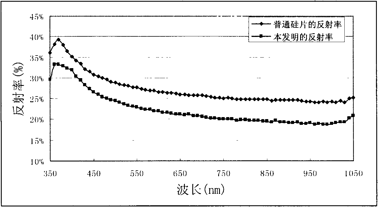
[0023] Mix hydrofluoric acid with a concentration of 17 mol / liter, potassium permanganate with a concentration of 0.01 mol / liter, and modifier sodium nitrite with a concentration of 0.1 mol / liter. The p-type polysilicon chip is soaked in the mixed acid etching solution. The etching temperature is 35° C., and the etching time is 15 minutes. After the etching is completed, the polysilicon wafer is immersed in a 1% NaOH solution and cleaned for 30 seconds. After cleaning, dry it and conduct a reflectivity test. For the test results, please refer to the attached figure 1 shown. It can be seen from the figure that, compared with common polysilicon wafers, the reflectance of the silicon wafers in this embodiment is lower in each wavelength band, with an overall decrease of about 8%.
Embodiment 2
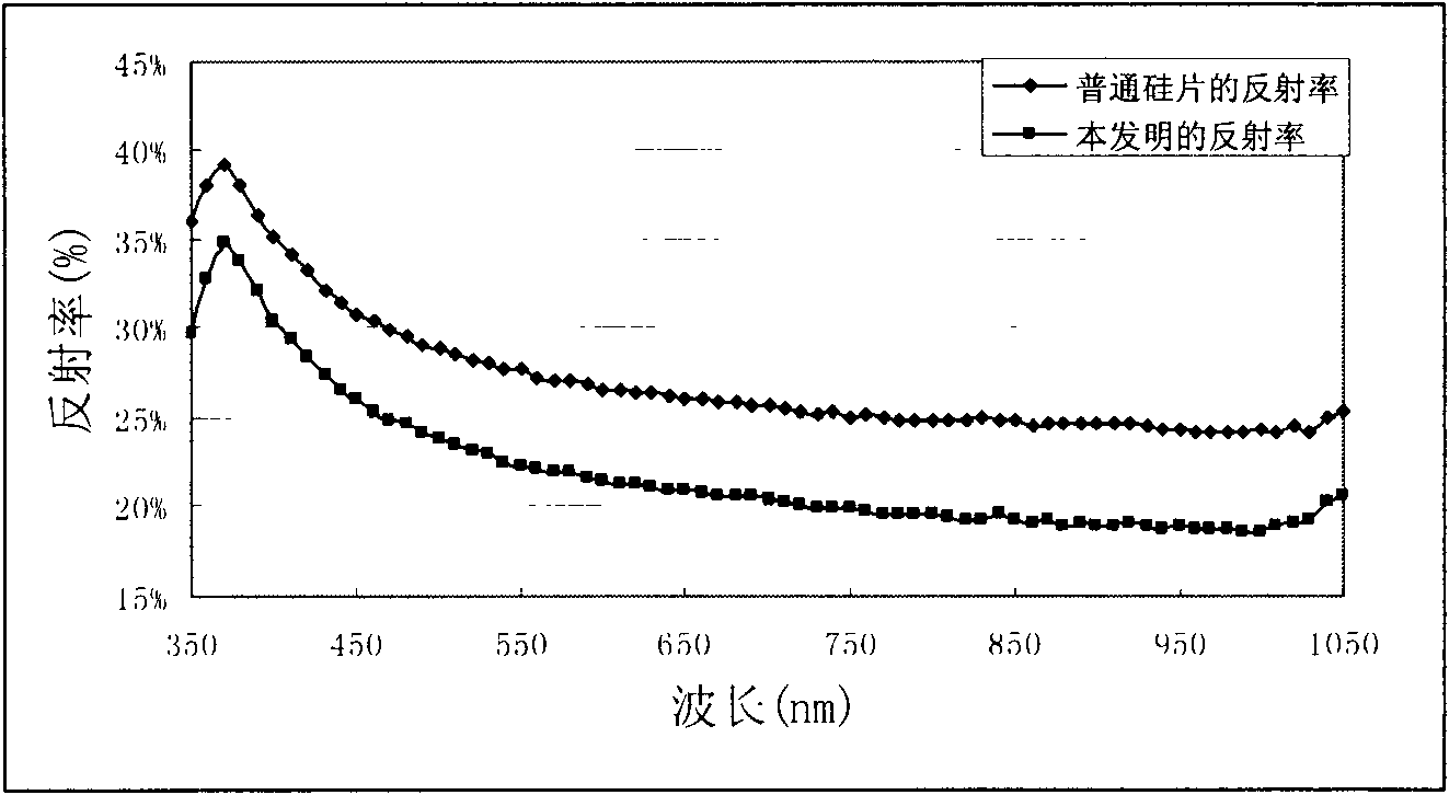
[0025] Mix hydrofluoric acid with a concentration of 13 moles / liter, potassium permanganate with a concentration of 0.05 moles / liter, and modifier sodium nitrite with a concentration of 0.2 moles / liter. The p-type polysilicon chip is soaked in the mixed acid etching solution. The etching temperature is 25° C., and the etching time is 35 minutes. After the etching is completed, the polysilicon wafer is immersed in a NaOH solution with a mass fraction of 1% and cleaned for 20 seconds. After cleaning, dry it and conduct a reflectivity test. For the test results, please refer to the attached figure 2 shown. It can be seen from the figure that, compared with common polysilicon wafers, the reflectivity of the silicon wafers in this embodiment is lower in each wavelength band.
Embodiment 3
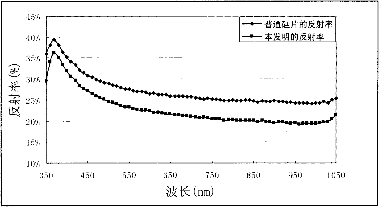
[0027] Mix hydrofluoric acid with a concentration of 15 mol / liter, potassium permanganate with a concentration of 0.4 mol / liter, and modifier sodium nitrite with a concentration of 0.15 mol / liter. The p-type polysilicon chip is soaked in the mixed acid etching solution. The etching temperature is 30° C., and the etching time is 30 minutes. After the etching is completed, the polysilicon wafer is immersed in a NaOH solution with a mass fraction of 1% and cleaned for 30 seconds. After cleaning, dry it and conduct a reflectivity test. For the test results, please refer to the attached image 3 shown. It can be seen from the figure that, compared with common polysilicon wafers, the reflectivity of the silicon wafers in this embodiment is lower in each wavelength band.
PUM
| Property | Measurement | Unit |
|---|---|---|
| thickness | aaaaa | aaaaa |
Abstract
Description
Claims
Application Information


