
Micro machine differential capacitance accelerometer with symmetrical structure

A technology of accelerometer and differential capacitance, which is applied in the direction of measuring acceleration, speed/acceleration/shock measurement, generator/motor, etc. It can solve the problems of performance degradation of accelerometer temperature characteristics, low bonding efficiency, and poor practicability, etc., to achieve Eliminate thermal mismatch stress, improve dynamic characteristics, and better anti-overload performance

Active Publication Date: 2010-01-13
安徽云芯微系统科技有限公司
View PDF3 Cites 28 Cited by
  • Summary
  • Abstract
  • Description
  • Claims
  • Application Information

AI Technical Summary

Problems solved by technology

Eric Peeters et al. used ordinary single crystal silicon wafers to control the thickness of the beam structure through concentrated boron diffusion and self-stop corrosion, which introduced a large stress, which would cause the temperature characteristics of the accelerometer to decline; in addition, the accelerometer’s The process has a fragile silicon substrate bonding process, which affects the yield of this accelerometer
[0006] In 2000, the Najafi research group of the University of Michigan made an all-silicon high-precision capacitive accelerometer. This accelerometer adopts a double-layer cantilever beam design, has a fully symmetrical structure, and is processed by a single single-crystal silicon wafer. , to achieve micro-g level acceleration detection, but the accelerometer adopts the concentrated boron diffusion self-stop corrosion process, which introduces a large stress, and the accelerometer has a fragile structure and poor practicability
[0007] The series of patents U.S.Pat.No.5484073; U.S.Pat.No.5652384; U.S.Pat.No.5852242; U.S.Pat.No. applied by I / O Sensors in the United States are successful solutions for high-precision micromachined accelerometers, but this solution Using two SOI wafers after deep etching for silicon-silicon bonding has the problems of high bonding risk, low bonding efficiency, and the reduction of sensitive structure symmetry caused by the inhomogeneity of the process results between the wafers during processing. problem, in addition, this scheme is difficult to achieve effective overload protection for non-sensitive axial

Method used


Image

  • Micro machine differential capacitance accelerometer with symmetrical structure
  • Micro machine differential capacitance accelerometer with symmetrical structure
  • Micro machine differential capacitance accelerometer with symmetrical structure

Examples


Embodiment 1

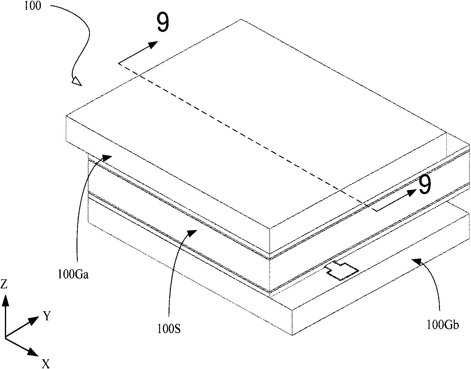
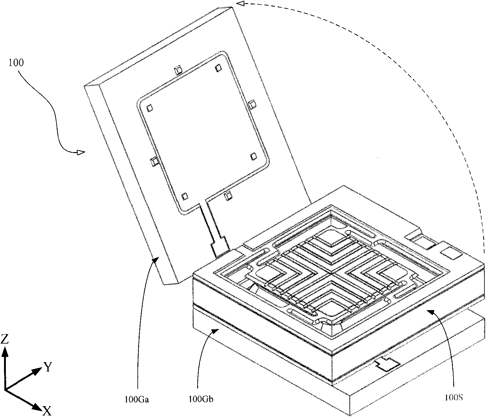
[0039] As shown in Figure 1-9, a micromechanical differential capacitive accelerometer with a symmetrical structure (glass electrode cover scheme). Figure 1A It is a frontal side view of the micromechanical differential capacitive accelerometer (glass electrode cover plan) according to the present invention. The accelerometer 100 of the glass electrode cover plan has a glass upper electrode cover plate 100Ga and a glass bottom electrode cover plate 100Gb , A silicon structural component 100S, Figure 1B It is an isometric side view of the 100 accelerometer with the upper glass electrode cover opened.

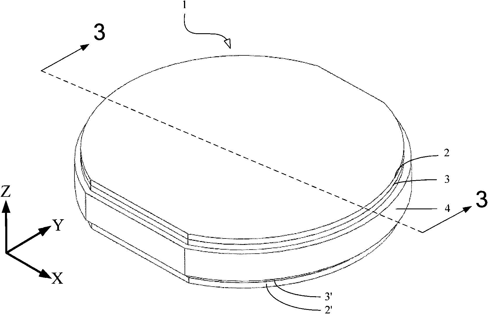
[0040] figure 2 It is the substrate 1 used to process the silicon structural component 100S, which is the front side view of a dual device layer SOI monocrystalline silicon wafer as described above, such as figure 2 As shown, this SOI wafer has a single crystal silicon lining 4, and the front and back sides of the single crystal silicon lining 4 have silicon dioxide insulating laye...

Embodiment 2

[0050] As shown in Figure 10-12, a micro-machined differential capacitance accelerometer with a symmetrical structure (single crystal silicon electrode cover plan). The monocrystalline silicon cover plan in this embodiment uses the same monocrystalline silicon structure component 100S as the glass electrode cover plan described in Example 1, except that monocrystalline silicon is selected as the electrode cover material, and the same structure is used The electrode cover plate made of glass material is different. Figure 10A Shown is a frontal side view of the monocrystalline silicon upper electrode cover 200Ga of the micromechanical differential capacitive accelerometer (single crystal silicon electrode cover scheme) 200 according to the present invention, Figure 10B It is an isometric side view of the back of the single crystal silicon upper electrode cover plate 200Ga. Since the single crystal silicon lower cover plate 200Gb and the single crystal silicon upper plate 200Ga ha...


PUM


Abstract

The invention relates to a micro machine differential capacitance accelerometer with a symmetrical structure, which is connected with a movable silicon structure component through an anchoring area along the upper direction and the lower direction. Elastic supporting beams of the silicon structure component are divided into an upper layer and a lower layer and distributed between a movable mass block and a fixedly supported frame as well as connected with the movable mass block and the fixedly supported frame; and the round angle transition is adopted at joints of the movable mass block and the fixedly supported frame as well as the beams; both the upper surface and the lower surface of the movable mass block are provided with gas flow guide grooves; and an electrode cover plate can be made of a silicon material. The gas flow guide grooves distributed on both the upper surface and the lower surface of the mass block are beneficial to regulating the squeeze-film damping effect of the accelerometer so as to structurally improve the dynamic characteristic of the surface separated capacitance detection accelerometer. A plurality of the elastic supporting beams of the accelerometer are made of single crystal silicon materials with a single doping concentration, thereby eliminating thermal inconsistency stress caused by adopting different materials and the thermal inconsistency stress caused by different single crystal silicon doping concentrations.

Description

Technical field [0001] The invention relates to a MEMS (micromachine, also known as microelectronic mechanical system) differential capacitance accelerometer capable of realizing high-precision detection of uniaxial acceleration, and in particular to a micromechanical differential capacitance accelerometer with a symmetrical structure, belonging to a capacitance accelerometer Technical field. Background technique [0002] Silicon single crystal material has good electrical properties and is the basic material of microelectronics technology. In addition, silicon also has good mechanical properties. Its breaking strength is three times that of stainless steel, its Knoop hardness is higher than stainless steel, and its elasticity is equivalent to stainless steel. MEMS technology is a kind of microelectronic three-dimensional processing technology developed after people have fully realized the outstanding electromechanical properties of single crystal silicon materials. Micro-senso...

Claims


Application Information

Patent Timeline
IPC IPC(8): G01P15/125B81B7/02
Inventor 高成臣胡启方郝一龙
Owner 安徽云芯微系统科技有限公司
Learn More