Method for etching class-III nitride by using photo-assisted oxidation wet method

A wet etching and nitride technology, which is applied in the fields of electrical components, semiconductor/solid-state device manufacturing, circuits, etc., can solve the problems of high ion energy and difficulty in obtaining etching mesa

Inactive Publication Date: 2010-01-13
INST OF SEMICONDUCTORS - CHINESE ACAD OF SCI
View PDF0 Cites 16 Cited by
  • Summary
  • Abstract
  • Description
  • Claims
  • Application Information

AI Technical Summary

Problems solved by technology

At present, most processes of group III nitrides use plasma dry etching, but in addition to many difficulties in production, dry etching also has many other defects. For example, the general energy of ions used in dry etching is low. It is very high, and it

Method used


Image

  • Method for etching class-III nitride by using photo-assisted oxidation wet method
  • Method for etching class-III nitride by using photo-assisted oxidation wet method
  • Method for etching class-III nitride by using photo-assisted oxidation wet method

Examples


Embodiment 1

[0033] In conjunction with accompanying drawing 1 (a), Fig. 1 (b), Fig. 1 (c), Fig. 1 (d) and figure 2 , the first embodiment of a method for wet etching Group III nitrides using photo-assisted oxidation of the present invention is described in detail as follows.

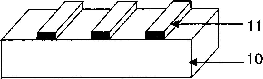
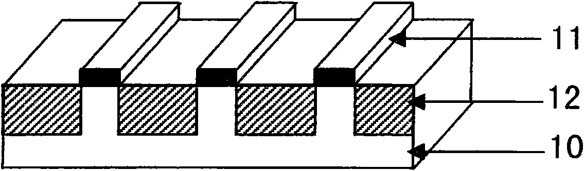
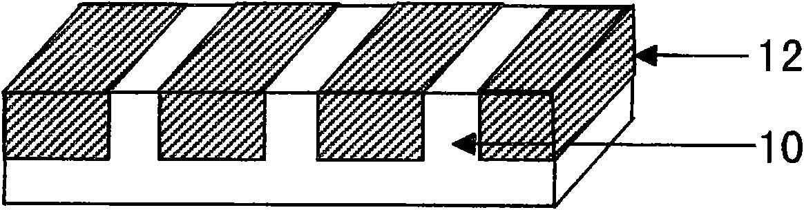
[0034] Step 1: Using a standard photolithography process, fabricate an ultraviolet light masking layer 11 with a certain pattern on the surface of the III-nitride sample 10 to be etched. The process includes baking the sample, cleaning the photoresist, coating the photoresist, baking the photoresist, exposing, developing, low-temperature coating, and stripping to form a pattern. The details are as follows: First, bake the III-nitride sample 10 at 120°C for 30 minutes, and then use a coater to evenly coat a layer of photoresist on its surface after it cools down, and then bake it at 90°C for 20 minutes. The photoresist has a certain hardness, and the photoresist is exposed by pattern exposure equipment, that is, a p...

Embodiment 2

[0040] In conjunction with accompanying drawing 1 (a), Fig. 1 (b), Fig. 1 (c), Fig. 1 (d) and image 3 , the second embodiment of a method for wet etching Group III nitrides using photo-assisted oxidation of the present invention is described in detail as follows.

[0041] Step 1, placing III-nitride sample 10 under a focused ultraviolet laser 34 for exposure (refer to image 3 ), the optical path is adjusted through the optical element group 35, the stepper motor 31 is precisely controlled by the computer control system 30 to move the sample, and the ultraviolet light switch 33 is used to realize the scanning exposure of the area to be exposed. The stepper motor can also be installed on the ultraviolet laser 34 to move the ultraviolet laser 34 or on the optical element group 35 to move the optical path, so as to realize the scanning exposure of the area to be exposed. The ultraviolet laser 34 may be a He—Cd laser or a frequency-doubled Ar+ laser or the like. The exposed are...

Embodiment 3

[0045] In conjunction with accompanying drawing 1 (a), Fig. 1 (b), Fig. 1 (c), Fig. 1 (d) and Figure 4 , the third embodiment of a method for wet etching Group III nitrides using photo-assisted oxidation of the present invention is described in detail as follows.

[0046] Step 1, at first adjust optical path, the light that makes ultraviolet laser 34 send is divided into two beams of coherent light beams after reflecting mirror 42 and half mirror 41 (referring to Figure 4 ). The two beams of coherent beams interfere on the surface of the III-nitride sample 10 after passing through two mirrors 40 respectively, forming alternate light and dark fringes. The ultraviolet laser 34 may be a He—Cd laser or a frequency-doubled Ar+ laser or the like.

[0047] Step 2. The group III nitride sample 10 is exposed under the light and dark ultraviolet light interference fringes. The ultraviolet light is strengthened, that is, the bright stripe area is oxidized under the assistance of ultr...


PUM


Abstract

The invention discloses a method for etching class-III nitride by using a photo-assisted oxidation wet method, which is characterized by comprising the following steps: step 1, preparing an ultraviolet light masking layer with patterns on the surface of the class-III nitride by using a standard photo-etching process; step 2, placing the class-III nitride of which the surface is provided with the ultraviolet light masking layer with the patterns under high-energy ultraviolet light to be exposed so as to oxidize the exposed class-III nitride with the patterns under the assistance of the ultraviolet light to generate a metal oxide; step 3, removing the masking layer; and step 4, putting a sample of the exposed class-III nitride in acid or alkali solution so that the generated metal oxide is fully eroded to form an etching step with the patterns to finish the process for etching the class-III nitride by the wet method.

Description

technical field [0001] The invention belongs to the technical field of semiconductor technology, specifically a method for etching group III nitrides (including GaN, AlN, InN and their ternary or multi-component compounds) by light-assisted oxidation wet method. Background technique [0002] Group III nitrides with direct band gaps (including GaN, AlN, InN and their ternary or multi-component compounds) are widely used in optoelectronics due to their wide spectral coverage, high electron saturation migration speed, good thermal conductivity and thermal stability. Devices and high-frequency high-power devices have attracted more and more attention. Etching is an unavoidable process in most device fabrication processes. Etching is to make steps such as dots, spots, lines, holes, grooves and other patterns on the surface of semiconductors. It is an indispensable process for the development of high-tech electronic devices. Circuit design plays an important role in studying the...

Claims


Application Information

Patent Timeline
IPC IPC(8): H01L21/302
Inventor 刘文宝孙苋赵德刚刘宗顺张书明朱建军杨辉
Owner INST OF SEMICONDUCTORS - CHINESE ACAD OF SCI
Why Eureka
Try Eureka