Multi-cell connected high-power photoelectric device with function of preventing single-cell thermoelectric damage
A photoelectric device, high-power technology, applied in the direction of electric solid-state devices, electrical components, semiconductor devices, etc., can solve the problems of uneven temperature distribution, reliability decline, uneven distribution, etc., to avoid hot spots or thermal collapse, Suppression of thermoelectric positive feedback effect, comprehensive effect of thermal reliability improvement
- Summary
- Abstract
- Description
- Claims
- Application Information
AI Technical Summary
Problems solved by technology
Method used
Image

Examples
Embodiment 1
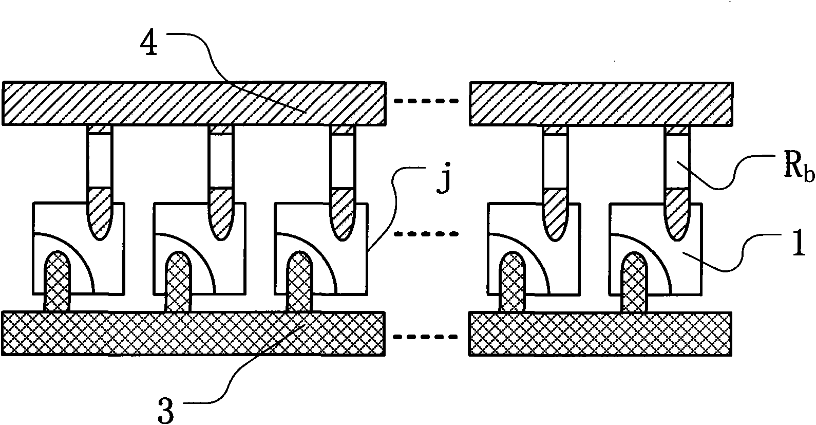
[0030] Such as Figure 2a The plane structure diagram of an ordinary front-emitting LED chip connected in series with ballast resistors connected in parallel is shown in the figure: the whole LED chip is composed of unit cell 1, ballast resistor 2, cathode lead 3, cathode pressure solder block 5, anode lead 4 and anode Composed of pressure welding blocks 6, wherein the cathode pressure welding block 5 and the anode pressure welding block 6 constitute the chip general lead-out electrode of the optoelectronic device. Each unit cell 1 is connected to the cathode welding block 5 through the cathode lead 3, and a ballast resistor 2 is connected in series on the anode lead 4 between the unit cell 1 and the anode welding block 6, and then connected to the anode welding block 6 . and Figure 2b Shown is a cross-section of a unit cell and its lead connection in a common front-emitting LED chip in which ballast resistors are connected in series and connected in parallel. The unit cel...
Embodiment 2
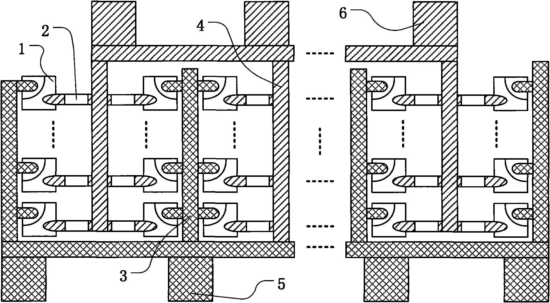
[0032] Such as Figure 3a As shown in the plane structure diagram of a vertical LED chip connected in series with ballast resistors in parallel: the whole LED chip consists of a unit cell active area 21, a ballast resistor 22, a cathode lead 23, a cathode solder block 24, and a conductive lining from the back. The composition of the anode drawn from the bottom. A ballast resistor 22 is connected in series on the cathode lead 23 between the unit cell active area 21 and the cathode welding block 24, and the unit cell active area 21, the ballast resistor 22 and the cathode welding block 24 are formed by the cathode lead 23 series access. and Figure 3b Shown is a cross-sectional structure of a unit cell and its lead connection in a vertical LED chip in which ballast resistors are connected in series and connected in parallel. The conductive substrate 20 is used for the anode extraction of the chip, the unit cell active region 21 is located on one side of the conductive substra...
Embodiment 3
[0034] The multi-cell parallel design with ballast resistors connected in series can also be applied to LED chips with a flip-chip structure, and its connection methods are also diverse.
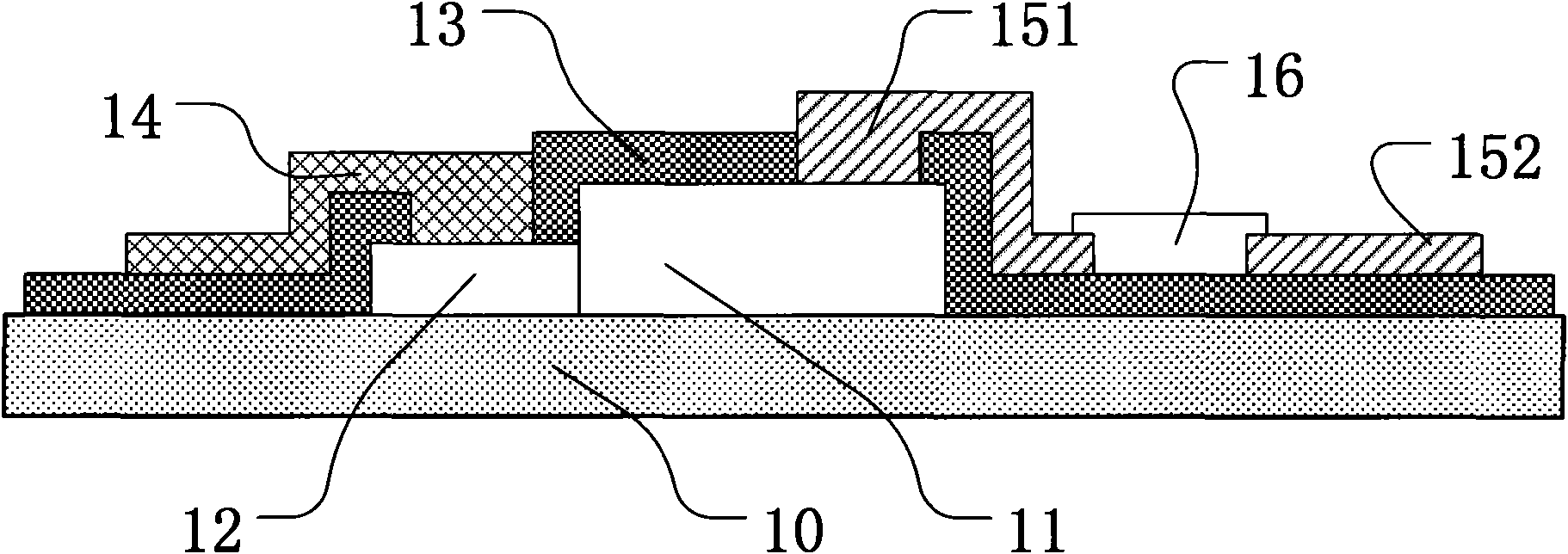
[0035] One of the connection methods is to design the ballast resistor on the same side as the active area of the LED chip. Such as Figure 4a As shown: the chip is composed of epitaxial substrate 30, active region 31, cathode lead-out region 32, insulating medium 33, cathode leads 341 and 342, anode bump 361 and cathode bump 371, while the transfer substrate is composed of anode bump 362, The cathode bump 372 , the anode lead 381 , the cathode lead 382 and the insulating substrate 39 are composed. The active chip and the transfer substrate are combined by a flip-chip welding process, the anode bump 361 is connected to the anode bump 362 , and the cathode bump 371 is connected to the cathode bump 372 . The current flows from the anode lead 381 to the active region through the anode bump ...
PUM
 Abstract
Description
Claims
Application Information
 - R&D
- Intellectual Property
- Life Sciences
- Materials
- Tech Scout
- Unparalleled Data Quality
- Higher Quality Content
- 60% Fewer Hallucinations
Browse by: Latest US Patents, China's latest patents, Technical Efficacy Thesaurus, Application Domain, Technology Topic, Popular Technical Reports.
© 2025 PatSnap. All rights reserved.Legal|Privacy policy|Modern Slavery Act Transparency Statement|Sitemap|About US| Contact US: help@patsnap.com