Multi-doping zinc-oxide-base wide-bandgap conducting material and preparation method thereof

A conductive material, zinc oxide-based technology, applied in the direction of conductive materials, conductive materials, cable/conductor manufacturing, etc., can solve problems such as easy performance degradation, unsatisfactory application, poor stability of single-doped zinc oxide-based films, etc. Achieve the effect of high transparent conductivity, high stability and high conductivity

Active Publication Date: 2010-03-03
山东中科泰阳光电科技有限公司
View PDF0 Cites 17 Cited by
  • Summary
  • Abstract
  • Description
  • Claims
  • Application Information

AI Technical Summary

Problems solved by technology

[0003] However, single-doped zinc oxide-based thin films such as BZO and AZO have poor stability and easy performance degradation in high-temperature and humid environments, which cannot meet the applications in solar cells and other optoelectronic fields.

Method used


Image

  • Multi-doping zinc-oxide-base wide-bandgap conducting material and preparation method thereof
  • Multi-doping zinc-oxide-base wide-bandgap conducting material and preparation method thereof

Examples


Embodiment 1

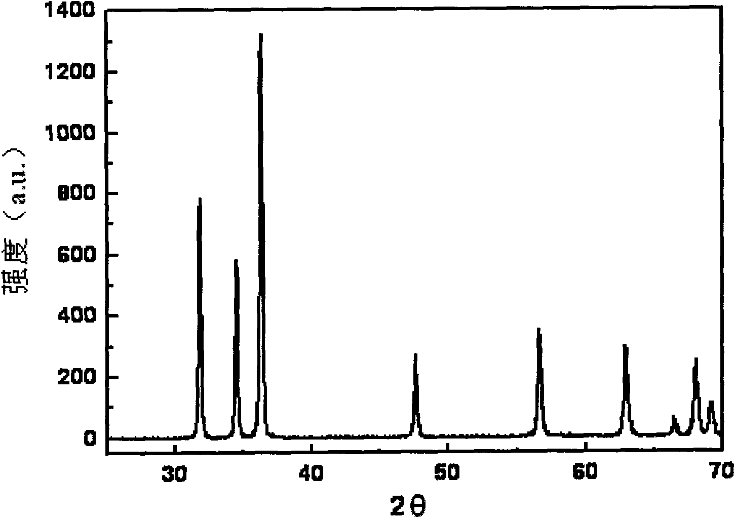
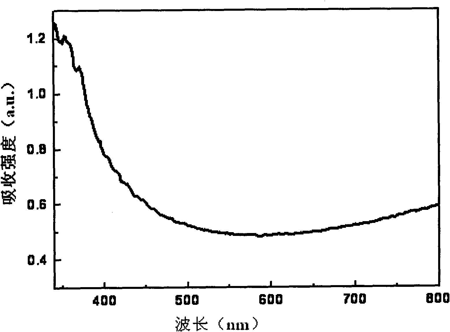
[0031]A preparation method of a multi-element doped zinc oxide (ZnO) wide bandgap conductive material, using zinc oxide, aluminum oxide and tin dioxide as raw materials, and the doping ratios of Al and Sn in terms of Zn are 2.0mol% and 1.0% respectively mol%, uniform ball milling and mixing for 20 hours to obtain the precursor doped powder, then pre-calcined at 900°C for 24 hours to obtain the doped powder, and finally compression molded and sintered at 1400°C for 4 hours to prepare ZnO:Al, Sn wide forbidden With conductive ceramic material. The material is 98% relative to the theoretical density, figure 1 It is the XRD spectrum of the ZnO:Al, Sn wide bandgap conductive ceramic material prepared in this embodiment, and the sample tested by XRD is a ZnO ceramic phase. figure 2 For the ZnO that makes in the present embodiment: Al, the absorption spectrum of Sn wide bandgap conductive ceramic material, illustrate that Al and Sn have been mixed in the ZnO lattice, have changed t...

Embodiment 2

[0035] A preparation method of a multi-element doped zinc oxide wide bandgap conductive material, using zinc oxide, aluminum hydroxide and ammonium tungstate as raw materials, and the doping ratios of Al and W based on Zn are 3.0 mol% and 0.25 mol% respectively , uniformly ball milled and mixed for 2 hours to obtain the precursor doped powder, then pre-fired at 800°C for 6 hours to obtain the doped powder, and finally compression molded and sintered at 1350°C for 12 hours to prepare ZnO:Al, W wide bandgap conductive Ceramic material.

[0036] Using the multi-element-doped zinc oxide wide-bandgap conductive material prepared in this example by high vacuum magnetron sputtering, the ZnO-based transparent conductive film has high visible light transmittance, and the temperature is 60 degrees Celsius 1. Accelerated aging for 50 hours in an environment with a relative humidity of 70% has a higher retention rate of more than 95% in electrical conductivity and light transmittance, and...

Embodiment 3

[0038] A preparation method of a multi-element doped zinc oxide wide bandgap conductive material, using zinc oxide, boric acid, aluminum hydroxide and gallium oxide as raw materials, and the doping ratios of B, Al and Ga are respectively 1.0 mol % and 1.0 mol % based on Zn. 3.0mol% and 0.25mol%, uniform ball milling and mixing for 2 hours to obtain a precursor doped powder, then pre-calcined at 800°C for 6 hours to obtain a doped powder, and finally compression molded and sintered at 1350°C for 12 hours to prepare ZnO: B, Al, Ga wide bandgap conductive ceramic material.

[0039] Using the multi-element-doped zinc oxide wide-bandgap conductive material prepared in this example by high vacuum magnetron sputtering, the ZnO-based transparent conductive film has high visible light transmittance, and the temperature is 60 degrees Celsius 1. Accelerated aging for 50 hours in an environment with a relative humidity of 70% has a higher retention rate of more than 95% in electrical cond...


PUM


Abstract

The invention belongs to the field of preparation of wide-bandgap conducting semiconductor materials, in particular to a multi-doping zinc-oxide-base wide-bandgap conducting material and a preparation method thereof. The multi-doping zinc-oxide-base wide-bandgap conducting material of the invention is prepared by mixing, drying, milling, presintering, die molding and sintering a dopant source anda zinc source. The high-performance zinc-oxide-base wide-bandgap conducting material has the advantages of simple process, low cost, high transparent conductivity, and high stability in high-temperature humid environment. The multi-doping zinc-oxide-base wide-bandgap conducting material can be used as a target material for preparing high-performance transparent conducting zinc-oxide films, and has wide application prospects in the fields of solar cells and photoconducting devices.

Description

technical field [0001] The invention belongs to the field of preparation of wide-bandgap conductive semiconductor materials, and in particular relates to a multi-doped zinc oxide-based wide-bandgap conductive material and a preparation method thereof. Background technique [0002] Transparent conductive oxide films are widely used in optoelectronic devices, such as touch screens for media terminals, flat liquid crystal displays (LCDs), solar cells, gas-sensitive devices, energy-saving windows, and anti-fog glass for automobiles. Indium trioxide and tin dioxide-based TCO (ITO, FTO) films are currently the most commonly used transparent conductive films. In recent years, with the rapid development of the optoelectronic device industry, the supply of TCO coated glass has been in short supply, especially in the field of thin film solar cells, the demand for high performance TCO thin films is more prominent. Due to the scarcity and cost of indium resources, the diffusion of heav...

Claims


Application Information

Patent Timeline
Patent Type & Authority Applications(China)
IPC IPC(8): H01B1/00H01B13/00H01B5/14C23C14/35C23C14/06H01L31/0224H01L31/18
CPCY02P70/50
Inventor 黄富强万冬云
Owner 山东中科泰阳光电科技有限公司
Why Eureka
Try Eureka