Aluminum gallium nitride/gallium nitride high electron mobility transistors

A high electron mobility, transistor technology, applied in circuits, electrical components, semiconductor devices, etc., can solve the problems of hysteresis of current and voltage output characteristics, device instability, permanent pollution of growth systems, etc.

Active Publication Date: 2010-05-26
THE HONG KONG UNIV OF SCI & TECH
View PDF0 Cites 35 Cited by
  • Summary
  • Abstract
  • Description
  • Claims
  • Application Information

AI Technical Summary

Problems solved by technology

Therefore, under high drain bias, electrons may be injected from the source to the high-field region through the GaN buffer layer, causing impact ionization in the channel, leading to three-terminal breakdown before the gate breakdown of the device
[0007] Although attempts have been made to reduce the n-type background doping in GaN buffer layers, such efforts have generally proven difficult and commercially unproductive
In addition, for example, carbon or Fe is doped into the GaN layer to form deep acceptor levels, but these acceptor levels are likely to cause the current collapse of the device and the hysteresis of the current-voltage (I-V) output characteristics, and the intentional introduction of impurities may also lead to Permanent contamination of the growing system
In addition, these acceptor impurities may also lead to device instability, especially when the drain operating voltage is high

Method used


Image

  • Aluminum gallium nitride/gallium nitride high electron mobility transistors
  • Aluminum gallium nitride/gallium nitride high electron mobility transistors
  • Aluminum gallium nitride/gallium nitride high electron mobility transistors

Examples


Embodiment Construction

[0049] Here, acronyms are used to represent the following, source (S), drain (D), gate (G), current (I), voltage (V), breakdown voltage (BV), transconductance (Gm), length, distance or spacing (L), relative position (X), ohmic contact (O), anode (A), cathode (C) or capacitance (C).

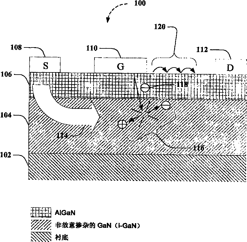
[0050] As mentioned earlier, the breakdown voltage values ​​of the currently reported AlGaN / GaN HEMTs are far below the theoretical limit of the material. From the current development level of AlGaN / GaN HEMT, due to the unintentional n-type background doping in the GaN buffer layer, the drain-induced barrier lowering (DIBL) effect is serious even in devices with a micron gate length.

[0051] figure 1 A schematic cross-section of a conventional AlGaN / GaN HEMT is shown along with a demonstration of device breakdown. AlGaN / GaN HEMTs are generally based on the epitaxial growth of GaN 104 (buffer layer) and AlGaN 106 (barrier layer) on a substrate material 102 (such as sapphire, silicon, silicon car...


PUM


Abstract

Structures, devices and methods are provided for creating enhanced back barriers that improve the off-state breakdown and blocking characteristics in aluminum gallium nitride AlGaN / GaN high electron mobility transistors (HEMTs). In one aspect, selective fluorine ion implantation is employed when developing HEMTs to create the enhanced back barrier structures. By creating higher energy barriers at the back of the two-dimensional electron gas channel in the unintentionally doped GaN buffer, higher off-state breakdown voltage is advantageously provided and blocking capability is enhanced, while allowing for convenient and cost-effective post-epitaxial growth fabrication. Further non-limiting embodiments are provided that illustrate the advantages and flexibility of the disclosed structures.

Description

technical field [0001] The invention belongs to field effect transistors, and particularly relates to improving the breakdown voltage of AlGaN / GaN high-mobility transistors and related materials, device structures and methods by using fluorine ion implantation. Background technique [0002] High Electron Mobility Transistor (HEMT), also known as Heterojunction Field Effect Transistor (HFET) or Modulation Doped Field Effect Transistor (MODFET), generally utilizes a junction formed by two materials with different band gaps, such as a heterojunction The replacement doped region acts as a channel. High electron mobility transistors benefit from heterostructures, taking advantage of the high-mobility electrons generated by heterojunctions made of, for example, highly doped wide-bandgap n-type donor layers or unintentionally doped AlGaN wide-bandgap layers and an undoped narrow bandgap layer (eg, a GaN layer) with little or no intentional dopant. [0003] For example, since a he...

Claims


Application Information

Patent Timeline
Patent Type & Authority Applications(China)
IPC IPC(8): H01L29/778H01L29/06H01L21/335H01L21/265
CPCH01L29/7788H01L29/207H01L29/2003H01L29/66462H01L29/7783
Inventor 陈敬王茂俊
Owner THE HONG KONG UNIV OF SCI & TECH
Why Eureka
Try Eureka