Method for manufacturing silicon photoelectric diode
A technology of silicon photodiodes and manufacturing methods, which is applied in the manufacture of circuits, electrical components, and final products, can solve the problems of unfavorable photoelectric measurement integration and miniaturization, increase device cost and installation complexity, and achieve reliability High, good repeatability and stability, simple process effect
- Summary
- Abstract
- Description
- Claims
- Application Information
AI Technical Summary
Problems solved by technology
Method used
Image

Examples
Embodiment Construction
[0024] The specific implementation of the present invention will be described below in conjunction with the accompanying drawings and technical solutions.
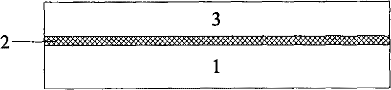
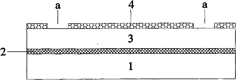
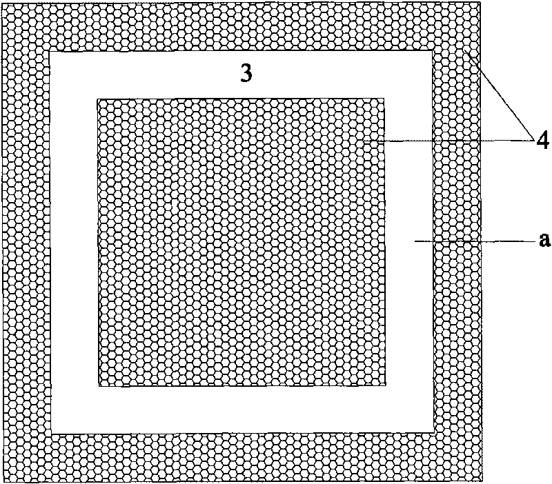
[0025] Firstly, select a suitable silicon-on-insulator wafer as a substrate, wherein selecting a device layer 3 with an appropriate thickness is the key. According to the Lambert-Beer theorem, the optical power in silicon decays exponentially with the increase of the incident depth, and the attenuation index is the absorption coefficient of the silicon material corresponding to the wavelength. Violet light is mainly absorbed in a very thin layer close to the surface of the silicon wafer, while long-wave light and near-infrared light in visible light, that is, the wavelength range of 500-1000 nanometers, can travel a relatively deep distance in silicon. We choose a silicon-on-insulator wafer as the substrate. The thickness of the device layer 3 of the wafer is generally less than 5 microns. This thickness range can ensure t...
PUM
| Property | Measurement | Unit |
|---|---|---|
| Thickness | aaaaa | aaaaa |
Abstract
Description
Claims
Application Information
 - Generate Ideas
- Intellectual Property
- Life Sciences
- Materials
- Tech Scout
- Unparalleled Data Quality
- Higher Quality Content
- 60% Fewer Hallucinations
Browse by: Latest US Patents, China's latest patents, Technical Efficacy Thesaurus, Application Domain, Technology Topic, Popular Technical Reports.
© 2025 PatSnap. All rights reserved.Legal|Privacy policy|Modern Slavery Act Transparency Statement|Sitemap|About US| Contact US: help@patsnap.com