Non-annular cavity type semiconductor laser

A ring cavity and semiconductor technology, used in semiconductor lasers, lasers, laser parts, etc., can solve the problems of reducing the electro-optical conversion efficiency of laser devices, reducing the optical output power of the device, and increasing the lasing threshold of the laser device. Conversion efficiency, the effect of improving optical output power

Inactive Publication Date: 2010-05-26
CHANGCHUN UNIV OF SCI & TECH
View PDF0 Cites 10 Cited by
  • Summary
  • Abstract
  • Description
  • Claims
  • Application Information

AI Technical Summary

Problems solved by technology

However, due to the adoption of this non-disc cavity structure, current injection will be performed on the entire disc-shaped area, while the whispering gallery mode of light only travels near the edge of the disc, and the current in the central part of the disc does not contribute to

Method used


Image

  • Non-annular cavity type semiconductor laser
  • Non-annular cavity type semiconductor laser
  • Non-annular cavity type semiconductor laser

Examples


Embodiment 1

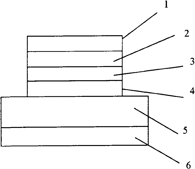
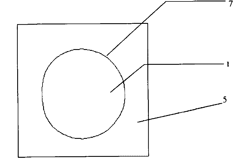
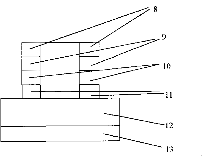
[0016] Such as Figure 3-4 As shown, the upper electrode 8 of the non-circular ring cavity is a gold electrode, the upper waveguide layer 9 is InGaAsP, the active gain region 10 is an InGaAs / InAlAs quantum well cascade structure, the lower waveguide layer 11 is InGaAsP, and the substrate 12 is InP And the lower electrode 13 is a gold electrode, the outer characteristic dimension R of the outer boundary 14 of the non-circular ring cavity 1 The radius is 100 microns, the deformation factor is 0.4, the emission wavelength of the device is 10 microns, and the inner feature size R of the inner boundary 15 of the non-circular ring cavity 2 It is 70 microns and the deformation factor is 0.4. The ring cavity is formed by reactive ion etching or wet etching. The inner and outer depths of the ring formed by the etching are the same, the active gain region 10 is exposed, the lower waveguide layer 11 is etched, and the substrate 12 is close. The lower electrode 13 of the non-circular ring ...

Embodiment 2

[0018] The inner boundary 15 of the non-circular ring cavity semiconductor laser is filled with insulating and heat-conducting material AlN; the others are the same as the first embodiment.

Embodiment 3

[0020] The upper electrode 8 of the non-circular ring cavity is a gold electrode, the upper waveguide layer 9 is InGaAsP, the active gain region 10 is an InGaAs / InAlAs quantum well cascade structure, the lower waveguide layer 11 is InGaAsP, the substrate 12 is InP and the lower electrode 13 is a gold electrode, the outer characteristic dimension R of the outer boundary of the non-circular ring cavity 14 1 The radius is 100 microns, the deformation factor is 0.4, the emission wavelength of the device is 10 microns, and the inner boundary 23 of the non-circular ring cavity is circular, such as Figure 5 As shown, the radius size is 70 microns, and the deformation factor is 0.4. The ring cavity is formed by reactive ion etching or wet etching. The inner and outer depths of the ring formed by the etching are the same, the active gain region 10 is exposed, the lower waveguide layer 11 is etched, and the substrate 12 is close. The lower electrode 13 of the non-circular ring cavity sem...


PUM


Abstract

The invention provides a non-annular cavity type semiconductor laser, adopting a non-annular cavity and comprising an upper electrode (8), an upper waveguide layer (9), an active gain region (10), a lower waveguide layer (11), a substrate (12) and a lower electrode (13) which are all non-annular and sequentially connected. The lower electrode (13) of the non-annular cavity type semiconductor laser is formed by welding solder on a copper heat sink, Compared with a non-circular dick cavity type semiconductor laser, the non-annular resonance cavity not only keeps optical orientation output, but also improves the current injection rate by more than 20%, decreases the lasing threshold of a laser device by more than 20%, improves the electro-optic conversion efficiency of the device by 15-20%, improves the optical output rate by 10-15% and overcomes the defects of the conventional structure. The laser can be applied to a semiconductor material system of an III-V group or a semiconductor material system of an II-VI group and can be also applied to organic fluorescent or laser material systems.

Description

Technical field [0001] The invention belongs to the field of semiconductor lasers and relates to a non-circular ring cavity semiconductor laser. Background technique [0002] Disc-shaped (micro) cavity semiconductor lasers are currently one of the most active research topics in the field of optoelectronics. Compared with edge-emitting semiconductor lasers, disc-shaped cavity semiconductor lasers have high quality factors, low lasing thresholds, and easy planar process preparation. The advantages of two-dimensional optical integration, so it has a wide range of application prospects in optical communication, optical interconnection and optical integration, etc., which has aroused people's great interest; the disadvantage of disc cavity semiconductor laser is that the optical output does not have a certain directionality , Along the boundary of the disc 360 degrees. Non-circular disc cavity semiconductor lasers are emerging representatives of this type of disc cavity semiconductor...

Claims


Application Information

Patent Timeline
IPC IPC(8): H01S5/00H01S5/10
Inventor 晏长岭邓昀冯源钟景昌
Owner CHANGCHUN UNIV OF SCI & TECH
Why Eureka
Try Eureka