Growing method of gallium nitride

A growth method, gallium nitride technology, applied in the field of gallium nitride epitaxy, can solve the problems of difficult to obtain high-quality device-grade gallium nitride materials and gallium nitride materials, and achieve low-cost and highly controllable growth Effect

Inactive Publication Date: 2010-06-09
INST OF SEMICONDUCTORS - CHINESE ACAD OF SCI
View PDF0 Cites 9 Cited by
  • Summary
  • Abstract
  • Description
  • Claims
  • Application Information

AI Technical Summary

Problems solved by technology

This method can obtain relatively good GaN materials on sapphire, SiC and even Si, but recent attempts have shown that it is difficult to obtain high-quality device-grade nitrogen in the growth of non-c-plane GaN by simply using a two-step method. gallium oxide material
In addition, it is difficult to grow gallium nitride materials on cheaper polycrystalline or amorphous substrates using a two-step method.

Method used


Image

  • Growing method of gallium nitride
  • Growing method of gallium nitride
  • Growing method of gallium nitride

Examples


Embodiment

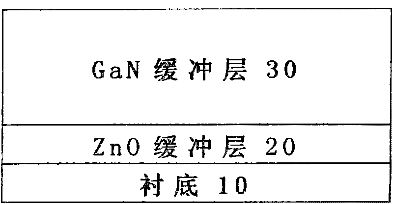
[0028] Please refer to figure 1 As shown, firstly, a zinc oxide buffer layer 20 is grown on the m-plane sapphire substrate 10 by magnetron sputtering, and the thickness of the buffer layer is 200nm. For comparison, we also choose not to grow the zinc oxide buffer layer 20 at the same time. The m-face sapphire was used for experimental control;

[0029] Then, a gallium nitride epitaxial layer 30 of 50 microns was grown on the sapphire with and without the zinc oxide buffer layer 20 grown by the HVPE method. In order to avoid the reaction of zinc oxide in a reducing atmosphere, nitrogen was used as the carrier gas;

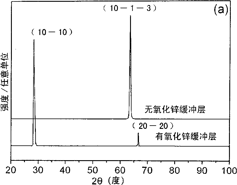
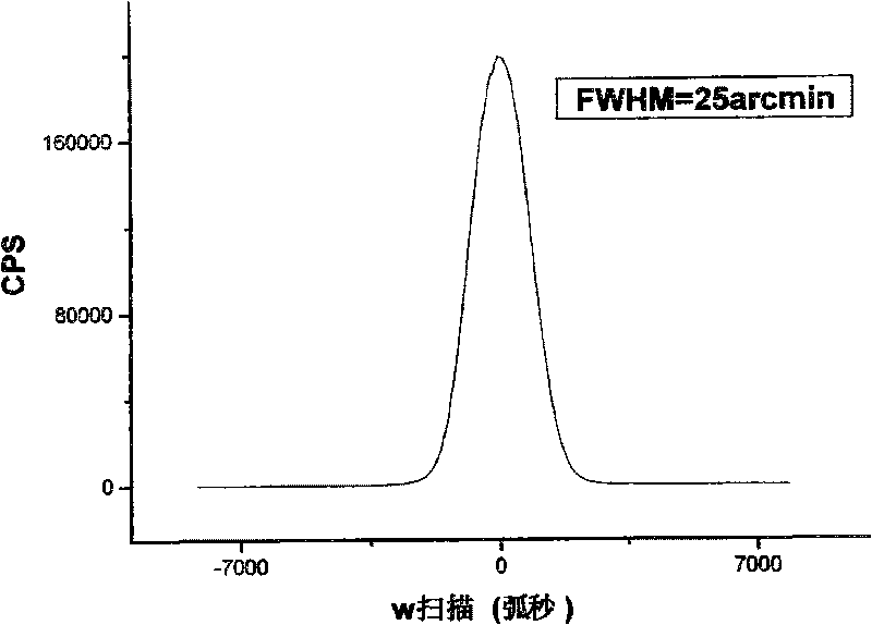
[0030] The grown gallium nitride was subsequently characterized by XRD, and it was found that the gallium nitride epitaxial layer 30 without the zinc oxide buffer layer 20 had a (10-1-3) plane orientation; while the gallium nitride grown with the zinc oxide buffer layer 20 The orientation of the epitaxial layer 30 is the m(10-10) plane orientation, (such as figur...


PUM

PropertyMeasurementUnit
thicknessaaaaaaaaaa
thicknessaaaaaaaaaa

Abstract

The invention relates to a growing method of gallium nitride. The growing method is characterized by comprising the following steps of: (1) getting a substrate; (2) growing a buffer layer by adopting methods of magnetron sputtering, pulsed laser deposition or metal organic chemical vapor deposition (MOCVD); and (3) growing an epitaxial layer on the buffer layer by adopting methods of MOCVD, high voltage paper electrophoresis (HVPE) or pulsed laser deposition and magnetron sputtering. The growing method of gallium nitride can realize the high-quality growth and the polarity selection of a gallium nitride material and the use of a low cost substrate.

Description

technical field [0001] The invention belongs to the technical field of semiconductors, and particularly refers to a growth method designed in combination with the growth of zinc oxide materials in the growth of gallium nitride materials, which can be used to realize the growth of high-quality non-polar gallium nitride and low-cost substrates GaN epitaxy on . Background technique [0002] Group III gallium nitride multi-system materials are semiconductor materials with direct bandgap, the bandgap can be continuously adjusted from 0.7eV to 6.2eV, and the color covers from infrared to ultraviolet wavelengths. In optoelectronics such as blue light, green light, and ultraviolet light-emitting diodes (LED ), short-wavelength laser diodes (LD), ultraviolet detectors, Bragg reflection waveguides, etc. have important applications and developments. In addition, gallium nitride (GaN) material, as one of the representatives of the third-generation semiconductor materials, has excellent...

Claims


Application Information

Patent Timeline
Patent Type & Authority Applications(China)
IPC IPC(8): H01L21/20C30B29/38C30B29/40
Inventor 段瑞飞魏同波王国宏曾一平李晋闽
Owner INST OF SEMICONDUCTORS - CHINESE ACAD OF SCI
Why Eureka
Try Eureka