Solar converter and compound converter

A converter, solar technology, applied in semiconductor devices, electrical components, circuits, etc., can solve problems such as conversion efficiency limitation, three-node limitation, low efficiency, etc.

Inactive Publication Date: 2010-06-09
NOVARTIS SPECTRUM
View PDF8 Cites 1 Cited by
  • Summary
  • Abstract
  • Description
  • Claims
  • Application Information

AI Technical Summary

Problems solved by technology

[0011] 1. The spectral range is limited to the bandgap of InGaP at 1.9 eV and the band gap of Ge at 0.65 eV
[0012] 2. The thickness of the multinode has limitations on absorbing all sub-micron photons in the concentrated beam
[0013] 3. The three material converters (gallium arsenide, germanium, indium gallium phosphide) converters have restrictions on the three materials
[0014] 4. This multi-node converter has a limit of three nodes
[0015] 5. The multi-node converter has limitations to the limited conversion efficiency provided by the crystal
[0016] 6. This node configuration has restrictions on flat configurations with nodes
[0017] 7. The incident angle of the sun beam has a limit to the normal plane incident angle
[0018] 8. This sunbeam has a limit to the gathering of less than 500 sunbeams
[0019] 9. The manufacturing process for manufacturing converters has limitations for high-volume, low-cost production; except for the production of large sheets of low-efficiency thin-film or organic solar converters

Method used


Image

  • Solar converter and compound converter
  • Solar converter and compound converter
  • Solar converter and compound converter

Examples


Embodiment Construction

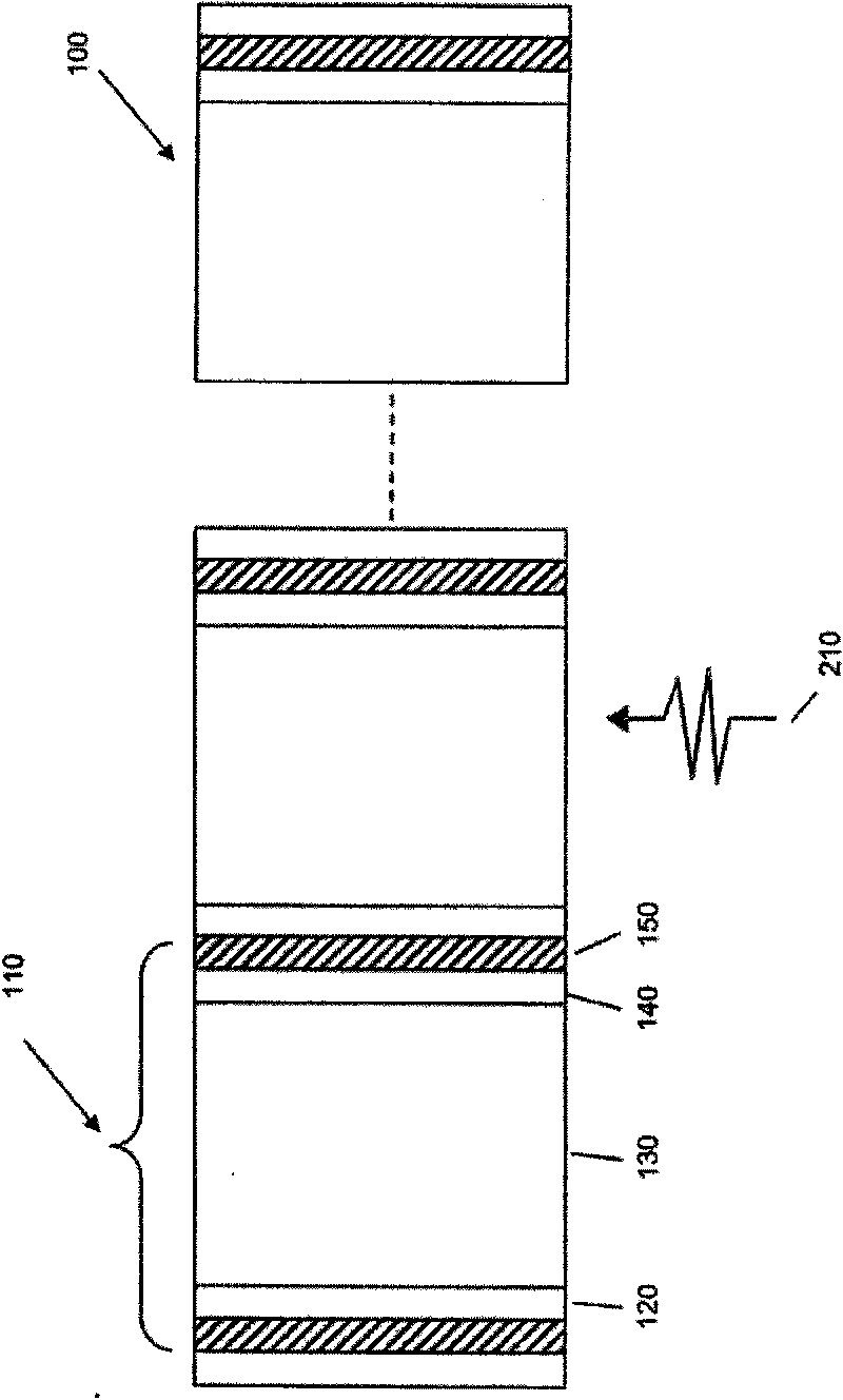
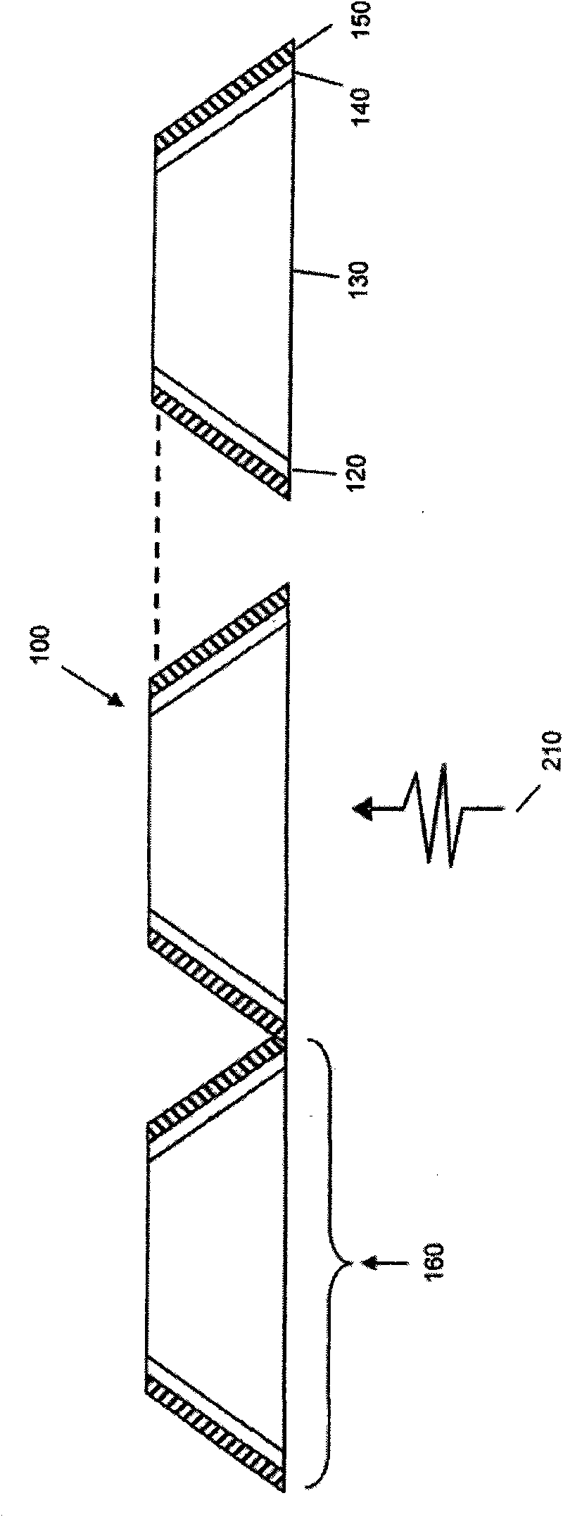
[0087] 1. Introducing the multi-node converter 100 .

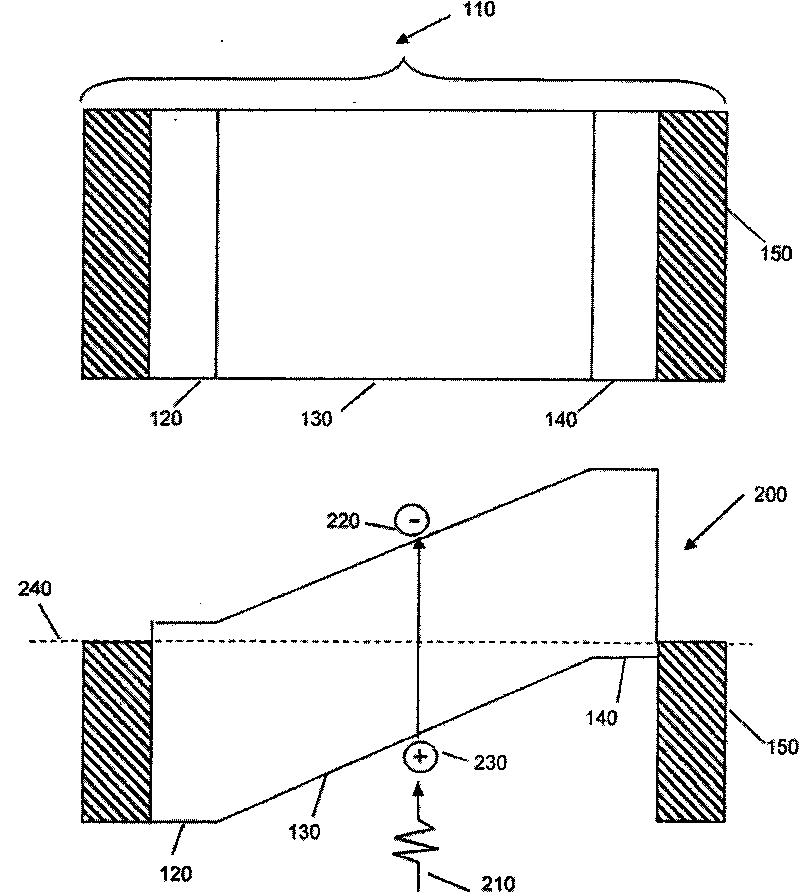
[0088] see Figure 1 to Figure 5 , the multi-node converter 100 may include one to thousands of photoelectric nodes 110, each photoelectric node 110 needs a hypertonic (10 19 / CM 3 ) n+ semiconductor layer 120, a low permeation (10 16 / CM 3 ) n-type high crystal semiconductor layer 130 and a hypertonic (10 19 / CM 3 ) p+ semiconductor layer 140 . A metal foil or eutectic metal layer 150 is formed between two adjacent n+ and p+ layers to reduce the overall series resistance of converter 100 .

[0089] As a preferred embodiment, making the multi-node converter 100 requires all nodes 110 to be electrically connected in parallel and in series so as to form an incremental voltage; refer to Figure 1 to Figure 5 .

[0090] The first component in this preferred embodiment is the node region and the doping layer of the multi-node converter 100; the node region and the doping layer have a high crystalline order in order to a...


PUM


Abstract

The invention relates to a multi-node multi-spectrum solar converter and a production method for converting solar energy into electric energy by using same. The solar converter is processed by diamond, aluminum arsenide, silicon, gallium phosphide, indium gallium phosphorus, gallium arsenide, germanium, silicon, indium gallium arsenic, indium carbide or any substrate sensitive to one or a plurality of solar spectrum zones and comprises one to thousands of parallel nodes illuminated by solar light. As an optimal embodiment, in order to obtain high converting efficiency, adjacent nodes are electrically connected by conductive layers for reducing serial resistance in the converter; a plurality of converters with different substrates of different band gaps are assembled into a compound converter. The compound converter has a multi-spectrum multi-node converting function and is used for converting the solar energy of the whole spectrum from ultraviolet ray to infrared ray.

Description

technical field [0001] The present invention relates to a multi-connected, multi-spectral conversion device and method of manufacture for converting solar energy into electrical energy, and in particular to a series of thousands of Apparatus and methods for converting concentrated beams of light into electrical energy through connected nodes of a meter. Background technique [0002] Multi-node, multi-spectrum solar energy converters are formed from three different semiconductor materials, gallium arsenide (GaAs), germanium (Ge), and indium gallium phosphide (InGaP), which are available at EMCORE Corporation (EMCORE, www.emcore.com, 2006) and the efforts of some other researchers have been further developed, and recently R. McConnell and other reports claim that it is "a new generation of optoelectronic technology in the United States"; The first European Photovoltaic Solar Energy Exhibition has overcome the difficulty of conversion efficiency of 38%; and reached an intentio...

Claims


Application Information

Patent Timeline
Patent Type & Authority Applications(China)
IPC IPC(8): H01L31/042H01L31/052H01L31/076
CPCY02E10/50Y02E10/548
Inventor 陈威廉
Owner NOVARTIS SPECTRUM
Why Eureka
Try Eureka