Manufacturing method of wafer level glass microcavity used for packaging MEMS

A manufacturing method, glass microtechnology, applied in the field of MEMS manufacturing, can solve problems such as complex methods, and achieve the effects of simple methods, good sphericity, and high molding height

Active Publication Date: 2010-06-16
SOUTHEAST UNIV
View PDF1 Cites 36 Cited by
  • Summary
  • Abstract
  • Description
  • Claims
  • Application Information

AI Technical Summary

Problems solved by technology

The method is m

Method used


Image

  • Manufacturing method of wafer level glass microcavity used for packaging MEMS
  • Manufacturing method of wafer level glass microcavity used for packaging MEMS
  • Manufacturing method of wafer level glass microcavity used for packaging MEMS

Examples


Embodiment 1

[0029] A method for manufacturing a wafer-level glass microcavity for MEMS packaging, comprising the following steps:

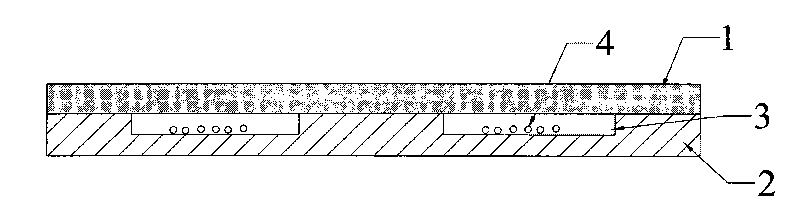
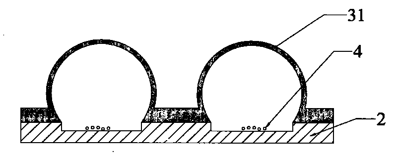
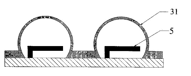
[0030]The first step utilizes Si micromachining process to etch shallow grooves on Si wafers (such as 4-inch wafers), and the silicon wafers used can be silicon wafers of standard thickness, such as 500 micron thick silicon wafers. The depth is 10-200 microns, such as 15 microns, 30 microns, 40 microns, 60 microns, 95 microns, 132 microns, 150 microns, 180 microns, and the aspect ratio is usually less than 2, such as 1.5, 1, 0.8, 0.5, 0.2, 0.1, 0.05, 0.02, the micromachining process of the pattern structure on the Si wafer is a wet etching process, or a dry inductively coupled plasma (ICP) etching process, or reactive ion etching, A wet etching process is preferred, such as etching with a TMAH solution, and the pattern can be a square or circular groove array (for packaging MEMS device arrays),

[0031] The second step is to place an appropriate amount of hi...

Embodiment 2

[0036] A method for manufacturing a wafer-level glass microcavity for MEMS packaging, comprising the following steps:

[0037] The first step is to use Si micromachining technology to etch shallow grooves on a 4-inch Si wafer. The silicon wafer used can be a standard thickness silicon wafer with a thickness of 500 microns. The depth of the shallow grooves is 60 microns. It is a circular groove of 2 mm, the micromachining process of the pattern structure on the Si wafer is a wet etching process, the etching solution used is TMAH solution, the concentration is 10%, and the temperature is 80 degrees Celsius.

[0038] In the second step, chemically pure calcium carbonate powder is placed in a shallow tank with a particle size of 5 microns and a mass of 2 micrograms.

[0039] The 3rd step, above-mentioned Si disc and Pyrex7740 glass disc (a kind of brand of borosilicate glass, the U.S. Corning-corning company produces, the market can buy, usually through polishing, its size is iden...

Embodiment 3

[0044] A method for manufacturing a wafer-level glass microcavity for MEMS packaging, comprising the following steps:

[0045] The first step is to use Si micromachining technology to etch shallow grooves on a 4-inch Si wafer. The silicon wafer used can be a silicon wafer of standard thickness with a thickness of 500 microns. The depth of the shallow grooves is 100 microns. It is a circular groove of 2 mm, the micromachining process of the pattern structure on the Si wafer is a wet etching process, the etching solution used is TMAH solution, the concentration is 10%, and the temperature is 80 degrees Celsius.

[0046] In the second step, chemically pure calcium carbonate powder is placed in a shallow tank with a particle size of 5 microns and a mass of 4 micrograms.

[0047] The 3rd step, above-mentioned Si disc and Pyrex7740 glass disc (a kind of brand of borosilicate glass, the U.S. Corning-corning company produces, the market can buy, usually through polishing, its size is ...


PUM


Abstract

The invention provides a manufacturing method of a wafer level glass microcavity used for packaging an MEMS, which comprises the following steps of: (1) etching a shallow slot on an Si wafer by an Si microfabrication process; (2) placing a right amount of high-temperature gas release agent in the shallow slot; (3) carrying out anodic bonding on the Si wafer and a Pyrex7740 glass wafer in air or vacuum and enabling the shallow slot on the Pyrex7740 glass to form a sealed cavity body; and (4) heating the bonded wafer in the air to the temperature of 810-890 DEG C, keeping the temperature for 3-5min, enabling molten glass corresponding to the sealed cavity body to be in a spherical shape by the high-temperature gas release agent because of positive pressure generated by gas generated by heating, cooling to the normal temperature, annealing and removing a silicon wafer to obtain a wafer level spherical glass microcavity array. The invention adopts the release of the high-temperature gas release agent to provide a gas source, is used for forming the glass microcavity and has the characteristics of low cost, simple method, high forming height and good degree of sphericity.

Description

technical field [0001] The invention relates to a MEMS (micro-electro-mechanical system) manufacturing technology, in particular to a method for manufacturing a wafer-level glass microcavity for MEMS packaging. Background technique [0002] In the field of MEMS manufacturing technology, Pyrex7740 glass (a glass containing alkaline ions, Pyrex is Corning's product brand) is an important material. It has a thermal expansion coefficient similar to that of Si materials, and has high light transmittance. High strength, and can form a high-strength bonding connection with the Si substrate by using the anodic bonding process, and a strong Si-O covalent bond is generated on the bonding surface, and its strength is even higher than that of the Si material itself. Due to such characteristics, Pyrex7740 glass is widely used in MEMS packaging, microfluidics and MOEMS (micro-optical electro-mechanical systems) and other fields. [0003] In the field of MEMS packaging, since devices gene...

Claims


Application Information

Patent Timeline
IPC IPC(8): B81C3/00
Inventor 尚金堂陈波寅张迪徐超柳俊文唐洁影黄庆安
Owner SOUTHEAST UNIV
Why Eureka
Try Eureka