Atomic layer deposition Al2O3/HfO2 method for regulating energy band offset between GaAs semiconductor and gate dielectric

An atomic layer deposition and gate dielectric technology, which is used in semiconductor/solid-state device manufacturing, semiconductor devices, electrical components, etc., and can solve the problems of small conduction band compensation, inability to effectively suppress gate leakage current, and low barrier height.

Inactive Publication Date: 2010-06-23
NANJING UNIV
View PDF0 Cites 21 Cited by
  • Summary
  • Abstract
  • Description
  • Claims
  • Application Information

AI Technical Summary

Problems solved by technology

However, the band gap of GaAs (1.46eV) is 0.34eV larger than that of Si (1.12eV), which may cause HfO 2 The conduction band compen

Method used


Image

  • Atomic layer deposition Al2O3/HfO2 method for regulating energy band offset between GaAs semiconductor and gate dielectric
  • Atomic layer deposition Al2O3/HfO2 method for regulating energy band offset between GaAs semiconductor and gate dielectric
  • Atomic layer deposition Al2O3/HfO2 method for regulating energy band offset between GaAs semiconductor and gate dielectric

Examples


Embodiment 1

[0029] 1) Substrate cleaning: The GaAs substrate was ultrasonically cleaned with acetone, ethanol, and isopropanol for 3 minutes to remove the oil on the GaAs surface, and then soaked in HCl aqueous solution for 3 minutes. The volume ratio of the HCl aqueous solution is HCl:H 2 O=1:10.

[0030] 2) Substrate passivation: clean the GaAs substrate with 8% volume ratio (NH 4 ) 2 Soak in S aqueous solution for 10 minutes to form Ga-S and As-S bonds on the surface of GaAs, and further remove excess As simple substance and As oxide;

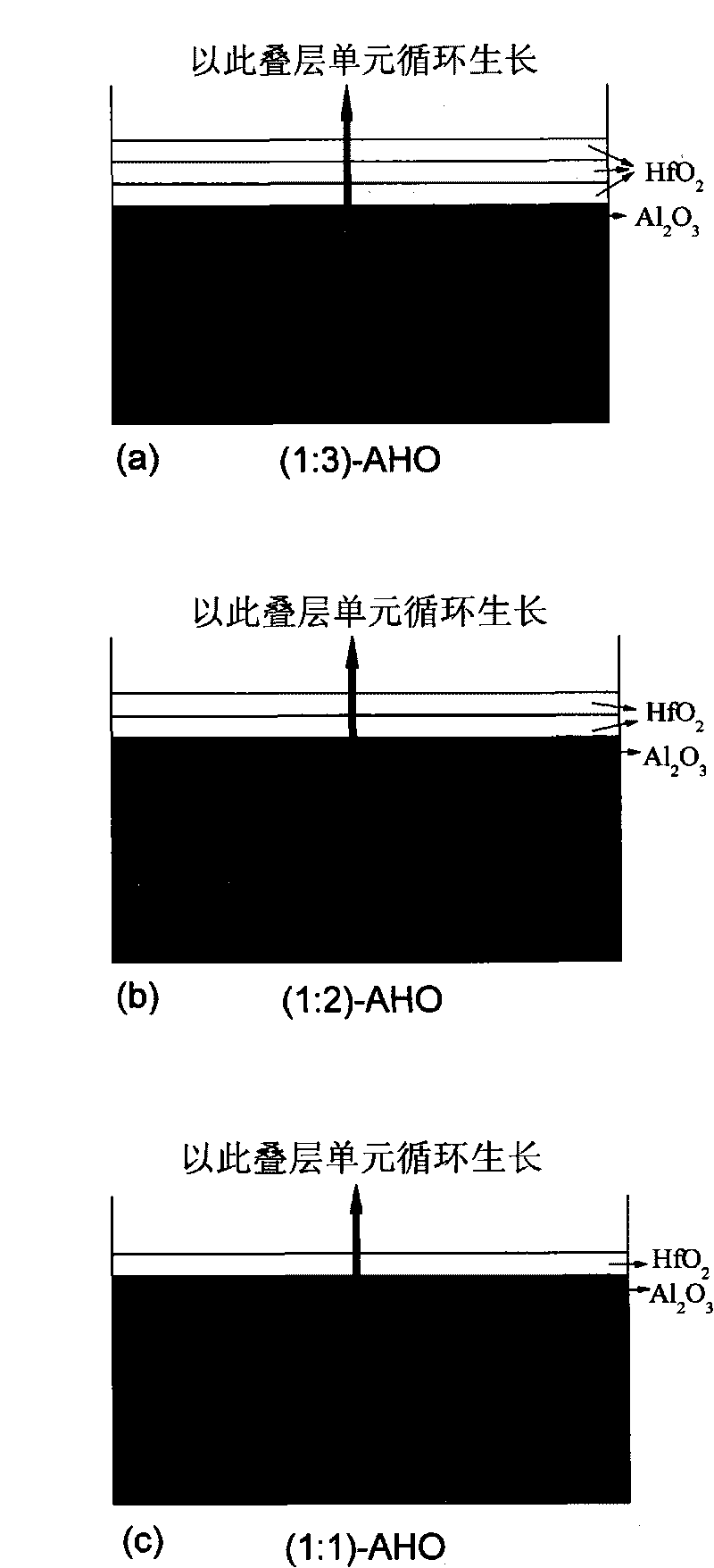
[0031] 3) Set the ALD deposition parameters: put the passivated GaAs substrate into the ALD reaction chamber immediately, and perform HfO 2 / Al 2 o 3 For the deposition of nano-laminated thin films, the ALD deposition parameters set are:

[0032] Reaction chamber temperature: 250°C;

[0033] Reaction source: deposited Al 2 o 3 Using Al(CH 3 ) 3 and H 2 O reaction; deposition of HfO 2 Using HfCl 4 and H 2 O reaction, where HfCl 4 The sourc...

Embodiment 2

[0037] 1) Substrate cleaning: ultrasonically clean the GaAs substrate with acetone, ethanol, and isopropanol for 10 minutes in order to remove the oil on the GaAs surface, and then soak it in HCl aqueous solution for 5 minutes. The volume ratio of the HCl aqueous solution is HCl:H 2 O=1:10.

[0038] 2) Substrate passivation: clean the GaAs substrate with 40% volume ratio (NH 4 ) 2 Soak in S aqueous solution for 40 minutes to form Ga-S and As-S bonds on the surface of GaAs, and further remove excess As simple substance and As oxide;

[0039] 3) Set the ALD deposition parameters: put the passivated GaAs substrate into the ALD reaction chamber immediately, and perform HfO 2 / Al 2 o 3 For the deposition of nano-laminated thin films, the ALD deposition parameters set are:

[0040] Reaction chamber temperature: 350°C;

[0041] Reaction source: deposited Al 2 o 3 Using Al(CH 3 ) 3 and H 2 O reaction; deposition of HfO 2 Using HfCl 4 and H 2 O reaction, where HfCl 4 The...

Embodiment 3

[0045] 1) Substrate cleaning: ultrasonically clean the GaAs substrate with acetone, ethanol, and isopropanol for 5 minutes in order to remove the oil on the GaAs surface, and then soak it in HCl aqueous solution for 4 minutes. The volume ratio of the HCl aqueous solution is HCl:H 2 O=1:10.

[0046] 2) Substrate passivation: clean the GaAs substrate with 25% volume ratio (NH 4 ) 2 Soak in S aqueous solution for 30 minutes to form Ga-S and As-S bonds on the surface of GaAs, and further remove excess As element and As oxide;

[0047] 3) Set the ALD deposition parameters: put the passivated GaAs substrate into the ALD reaction chamber immediately, and perform HfO 2 / Al 2 o 3 For the deposition of nano-laminated thin films, the ALD deposition parameters set are:

[0048] Reaction chamber temperature: 300°C;

[0049] Reaction source: deposited Al 2 o 3 Using Al(CH 3 ) 3 and H 2 O reaction; deposition of HfO 2 Using HfCl 4 and H 2 O reaction, where HfCl 4 The source te...


PUM


Abstract

The invention discloses an atomic layer deposition Al2O3/HfO2 method for regulating an energy band offset between a GaAs semiconductor and a gate dielectric. The method comprises the following steps of: firstly, cleaning a GaAs substrate to remove oil stains and oxide layers; secondly, immersing the cleaned GaAs substrate in aqueous solution of (NH4)2S to form Ga-S and As-S bonds on the surface of the GaAs substrate and further remove an unnecessary As elementary substance and As oxides; and finally, placing the passivated GaAs substrate into an ALD reaction chamber immediately to perform deposition of a HfO2/Al2O3 nano laminated film. The method optimizes and improves the interface property between the gate dielectric and the GaAs substrate, regulates the energy band offset between n-GaAs and a gate dielectric film, and improves the electrical properties of the gate dielectric film by changing the Al/Hf proportion, and has the advantages of simple process and important application prospect in preparation of GaAs-based MOSFETs.

Description

technical field [0001] The invention relates to atomic layer deposition technology, in particular to an atomic layer deposition of HfO on a GaAs substrate 2 / Al 2 o 3 A method for adjusting the energy band compensation between the semiconductor and the gate dielectric with a nano-stack structure. Background technique [0002] High dielectric constant gate dielectric HfO 2 The material has replaced traditional silicon dioxide and has been successfully used in silicon-based microprocessor chips of Intel's 45nm node. Although a lot of progress has been made in the research of high dielectric materials in the field of traditional silicon-based integrated circuits, there are still a series of challenges. One of the main problems is the introduction of high-k gate dielectric and metal gate material. While reducing the high power consumption of small-scale complementary CMOS devices, it also brings about the deterioration of the channel material / gate dielectric material interfa...

Claims


Application Information

Patent Timeline
IPC IPC(8): H01L21/28H01L21/285H01L21/336
Inventor 龚佑品李爱东刘晓杰吴迪
Owner NANJING UNIV
Why Eureka
Try Eureka