Gallium nitride based schottky diode with field plate structure

A Schottky diode, gallium nitride-based technology, applied in the direction of electrical components, circuits, semiconductor devices, etc., can solve the problem of low breakdown voltage, achieve capacitance increase per unit area, large reverse breakdown voltage, improve reverse effect on withstand voltage characteristics

Inactive Publication Date: 2010-06-23
NANJING UNIV
View PDF0 Cites 20 Cited by
  • Summary
  • Abstract
  • Description
  • Claims
  • Application Information

AI Technical Summary

Problems solved by technology

[0008] The object of the present invention is: to propose a GaN-based Schottky diode device structure using a high dielectric constant material as a field plate dielectric layer, in

Method used


Image

  • Gallium nitride based schottky diode with field plate structure
  • Gallium nitride based schottky diode with field plate structure
  • Gallium nitride based schottky diode with field plate structure

Examples


Embodiment Construction

[0028] In order to make the technical solutions and effects of the present invention clearer, the present invention will be further described below in conjunction with specific embodiments and with reference to the accompanying drawings. The same numbered parts in the various drawings represent the same device constituent parts or materials.

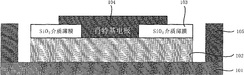
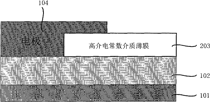
[0029] figure 1 Shown is a schematic cross-sectional structure of a conventional GaN-based power Schottky diode with a field plate structure. The basic building blocks of the device include:

[0030] The ohmic contact layer 101 is generally a heavily doped GaN layer, and its basic feature is that the N-type doping concentration is greater than 5×10 17 Per cubic centimeter, the thickness is between 0.2-20 microns. The ohmic contact layer 101 is generally deposited on a substrate material, and common substrate materials include: sapphire (Al 2 O 3 ), silicon (Si), silicon carbide (SiC), gallium arsenide (GaAs) or GaN bulk material su...


PUM

PropertyMeasurementUnit
Thicknessaaaaaaaaaa
Thicknessaaaaaaaaaa
Doping concentrationaaaaaaaaaa

Abstract

The invention discloses a gallium nitride based schottky diode with a field plate structure, wherein the periphery of a schottky metal electrode is provided with a layer of an insulating medium film, and the schottky metal electrode is extended to the upward side of the insulating medium film and covers part of the insulating medium film, namely a circle of metal-insulating medium layer-semiconductor (MIS) field plate structure is formed on the periphery of the schottky metal electrode; and the insulating medium layer of the field plate structure comprises at least one layer of an insulating material with a high dielectric constant, the thickness of the insulating material is between 0.01 and 2 microns, and the dielectric constant is bigger than 6. The gallium nitride based schottky diode comprises an ohmic contact layer, a GaN active layer, an insulating medium field plate, the schottky metal electrode and an ohmic contact electrode. Compared with a conventional structure device, a rectifier using the GaN schottky diode provided with the high dielectric constant material field plate has evener electric field distribution and higher reverse breakdown voltage.

Description

technical field [0001] The present invention relates to the technical field of power rectifier devices based on wide bandgap compound semiconductor materials, in particular to a gallium nitride-based Schottky diode device using an insulating material with a high dielectric constant as a field plate dielectric layer. Background technique [0002] Power electronic devices such as power rectifiers and power switches are widely used in various fields of the national economy, such as switching power supplies, automotive electronics, radio communications, motor control, etc. Silicon-based power electronic devices have been used for a long time; however, with the development of silicon technology for many years, the performance of corresponding silicon-based power electronic devices has gradually approached its theoretical limit. In order to greatly improve device performance and break through the "silicon limit" problem faced by the development of power electronic devices, new sem...

Claims


Application Information

Patent Timeline
IPC IPC(8): H01L29/872
Inventor 陆海石宏彪修向前陈鹏张荣郑有炓
Owner NANJING UNIV
Why Eureka
Try Eureka