Preparation method of c-axis inclined AlN thin film with homogeneous buffer layer

A technology for thin film preparation and buffer layer, applied in coating, metal material coating process, ion implantation plating, etc., can solve the problems of poor controllability of c-axis inclination angle, large lattice mismatch, etc., and achieve smooth surface and structure. dense effect

Inactive Publication Date: 2010-07-14
HUBEI UNIV
View PDF0 Cites 18 Cited by
  • Summary
  • Abstract
  • Description
  • Claims
  • Application Information

AI Technical Summary

Problems solved by technology

[0003] The purpose of the present invention is to provide a method for preparing a c-axis tilted AlN film with a homogeneous buffer layer, which can ov

Method used


Image

  • Preparation method of c-axis inclined AlN thin film with homogeneous buffer layer
  • Preparation method of c-axis inclined AlN thin film with homogeneous buffer layer
  • Preparation method of c-axis inclined AlN thin film with homogeneous buffer layer

Examples


Embodiment 1

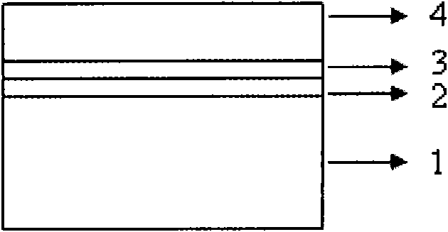
[0027] The specific steps for growing a c-axis tilted AlN film after depositing metal molybdenum (Mo) on a p-type (100) crystal-oriented Si substrate are as follows (combined with reference to the figure):

[0028] 1. Select a p-type (100) crystal-oriented Si substrate (1) deposited with a layer of 100nm metal molybdenum (2), and wash it with acetone, absolute ethanol and deionized water in sequence;

[0029] 2. Fix the Si substrate (1) on the turntable carrying the substrate holder, put it into the reaction chamber of the magnetron sputtering instrument, use 99.999% high-purity Al as the target material, and pump the reaction chamber to a vacuum degree of 0.4mPa;

[0030] 3. Introduce argon gas to make the pressure of the vacuum chamber reach 5Pa, pre-sputter the Al target for 10 minutes, remove the naturally generated oxide layer on the surface of the Al target, control the substrate temperature at 300°C, and inject N 2 , so that the air pressure in the vacuum chamber is 10P...

Embodiment 2

[0036] The specific steps for growing a c-axis tilt-oriented AlN film after depositing metal platinum (Pt) on a p-type (100) crystalline silicon substrate are as follows (combined with reference to the figure):

[0037] 1. Select a p-type (100) crystal-oriented Si substrate (1) deposited with a layer of 100nm metal platinum (2), and wash it with acetone, absolute ethanol and deionized water in sequence;

[0038] 2. Fix the Si substrate (1) on the turntable carrying the substrate holder, put it into the reaction chamber of the magnetron sputtering instrument, use 99.999% high-purity Al as the target material, and pump the reaction chamber to a vacuum degree of 0.4mPa;

[0039] 3. Introduce argon gas to make the pressure of the vacuum chamber reach 5Pa, pre-sputter the Al target for 10 minutes, remove the naturally generated oxide layer on the surface of the Al target, control the substrate temperature at 300°C, and inject N 2 , so that the air pressure in the vacuum chamber is ...

Embodiment 3

[0044] The specific steps for growing a c-axis oblique orientation AlN film after depositing metal gold (Au) on a p-type (100) crystal-oriented Si substrate are as follows (combined with reference to the figure):

[0045] 1. Select a p-type (100) crystal-oriented Si substrate (1) deposited with a layer of 100nm metal gold (2), and wash it with acetone, absolute ethanol and deionized water in sequence;

[0046]2. Fix the Si substrate (1) on the turntable carrying the substrate holder, put it into the reaction chamber of the magnetron sputtering instrument, use 99.999% high-purity Al as the target material, and pump the reaction chamber to a vacuum of 0.4mPa

[0047] 3. Introduce argon gas to make the pressure of the vacuum chamber reach 5Pa, pre-sputter the Al target for 10 minutes, remove the naturally generated oxide layer on the surface of the Al target, control the substrate temperature at 300°C, and inject N 2 , so that the air pressure in the vacuum chamber is 10Pa;

[0...


PUM


Abstract

The invention provides a preparation method of a c-axis inclined AlN thin film with homogeneous buffer layer, which comprises the steps that: generating an uncrystallized AlN thin film buffer layer on a substrate which is made from Si, Mo, Pt and Au or combination thereof by means of magnetron sputtering; and generating a c-axis oriented AlN thin film with different inclination degrees by adjusting the deviation angle between the substrate and the center of a target material. The preparation method can overcome the problems that the lattice mismatch between the AlN thin film and the substrate such as Si and GaAs, and the like, is larger, and the control performance of the c-axis inclination degree is worse. When being taken as a piezoelectric layer of a piezoelectric resonance sensor, the AlN thin film generated by the method can reduce the energy consumption of sound wave in liquid and is good for improving the quality factor and the sensitivity of the sensor.

Description

technical field [0001] The invention relates to the technical field of semiconductors, in particular to a method for preparing a c-axis inclined AlN thin film. Background technique [0002] Since the first-generation silicon semiconductor materials and the second-generation gallium arsenide semiconductor materials tend to be limited in device applications, AlN, as a representative of the third-generation direct wide bandgap semiconductor materials, has high thermal conductivity, high hardness, high melting point and chemical The characteristics of high stability, strong breakdown field and low dielectric loss, especially the similar thermal expansion coefficient of AlN and Si, GaAs and other commonly used semiconductor materials and strong growth process compatibility, have attracted great attention. In addition, among all inorganic nonferrous piezoelectric materials, the transmission speed of sound waves along the c-axis direction of AlN crystal is the largest. Therefore, ...

Claims


Application Information

Patent Timeline
IPC IPC(8): C23C14/34C23C14/58
Inventor 顾豪爽熊娟吴雯杜鹏飞胡明哲陈侃松
Owner HUBEI UNIV
Why Eureka
Try Eureka