Liquid crystal display array base plate and patching method thereof

A liquid crystal display and array substrate technology, applied in the field of liquid crystal display array substrates, can solve the problems of increasing the difficulty of the manufacturing process, increasing the complexity of the pixel structure, and not being able to achieve better repair effects, etc.

Active Publication Date: 2010-07-14
CENTURY DISPLAY (SHENZHEN) CO LTD
View PDF6 Cites 28 Cited by
  • Summary
  • Abstract
  • Description
  • Claims
  • Application Information

AI Technical Summary

Problems solved by technology

Although this method can achieve the repair of broken lines, the repair procedure is relatively cumbersome, and when depositing the metal film 41, the deposition time may be longer, and the film formation effect cannot be guaranteed, and the pixel electrode may be polluted during the deposition process. thereby affecting the quality of the picture
[0008] To sum up, the method of repairing data line defects in the prior art cannot achieve a good repair effect. If the method of the prior art is used for repair, it will not only increase the complexity of the pixel structure, but also increase the corresponding The manufacturing process is difficult, and it is more likely to pollute the pixel electrodes; therefore, it is necessary to propose a repair method that is simpler and does not generate other defects during the repair process. The present invention will propose a repair method that is simpler and has a better repair effect. good laser repair

Method used


Image

  • Liquid crystal display array base plate and patching method thereof
  • Liquid crystal display array base plate and patching method thereof
  • Liquid crystal display array base plate and patching method thereof

Examples


Embodiment Construction

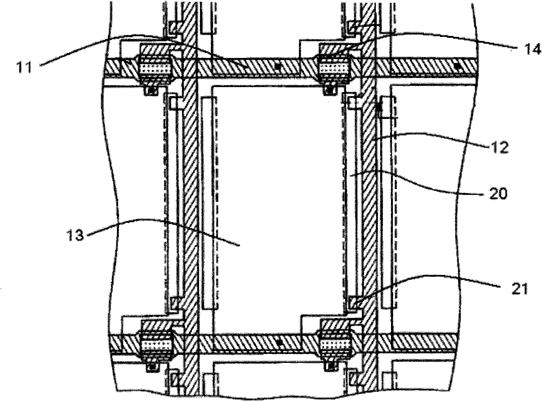
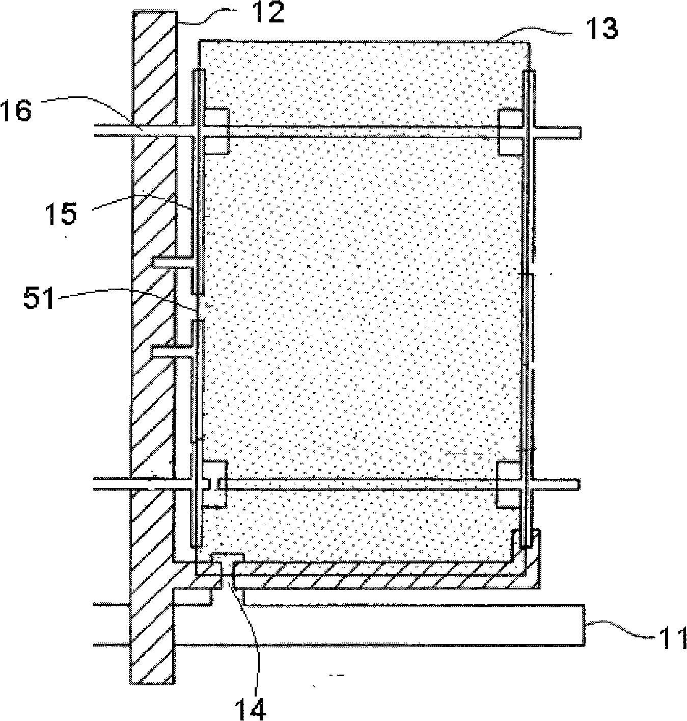
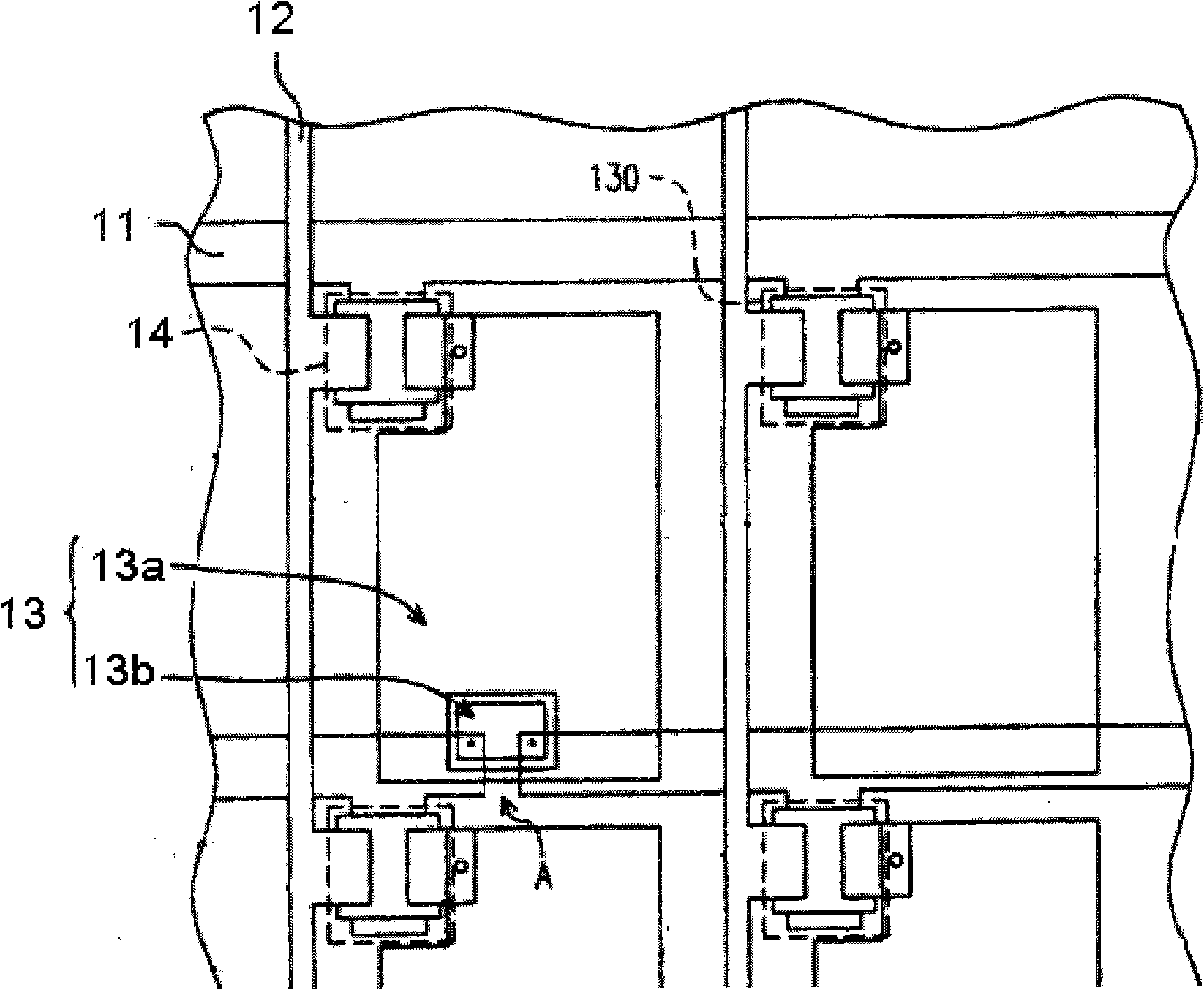
[0040] In the method and structure described in the following embodiments, the line defect of the data line or the scan line can be repaired, and the repair line can be designed without occupying the pixel aperture ratio.

[0041] Figure 4 It is a schematic diagram of the disconnection repair process of the present invention. refer to Figure 4 As shown, first put a liquid crystal display array substrate (S01) and then detect the missing line and determine the position of the line defect (S02). The detection system is detected by AOI machine or other detectable methods / machines such as TESTER machine The line defect of the signal transmission line, the above-mentioned signal transmission line includes a data line and a scanning line, then determine the position of the line defect on the data line or scanning line, and remove the barrier layer extending from the two ends of the line defect position to the common electrode line (S03), Here, the position of the barrier layer i...


PUM


Abstract

The invention provides a a patching method of a liquid crystal display array base plate. The patching method comprises the following patching flow processes: firstly, providing the liquid crystal display array base plate; then, detecting a linear defect part and simultaneously determining the position of the linear defect; next, using laser light beams for removing baffle layers formed by extending the two adjacent ends of the linear defect to a common electrode line; then, using a laser chemical deposition method for depositing a connection metal layer on the baffle layer removing position; finally, cutting off the adjacent external end electric connection part of the baffle layer on the common electrode line through laser light beams; and then, making a signal transmission line of the linear defect be able to complete the signal transmission through the common electrode line section. Thereby, the restoration method can effectively restore the defect of the signal transmission line on the original design, and the generation of other adverse defects caused by design modification can be avoided.

Description

【Technical field】 [0001] The invention relates to an array substrate of a liquid crystal display, in particular to an array substrate of a liquid crystal display capable of repairing line defects and a repairing method thereof. 【Background technique】 [0002] At present, the use of liquid crystal displays has become a trend. Liquid crystal displays have superior characteristics such as high image quality, better space utilization, low power consumption, and no radiation. With the increasingly mature technology of liquid crystal displays, liquid crystal displays are widely used applied to various fields. Generally speaking, a liquid crystal display is mainly composed of an array substrate, a pair of facing substrates and a liquid crystal layer sandwiched between the two substrates. Wherein, the array substrate mainly includes a substrate, pixel structures arranged in an array on the substrate, scanning lines and data lines. The aforementioned pixel structure is mainly compo...

Claims


Application Information

Patent Timeline
Patent Type & Authority Applications(China)
IPC IPC(8): G02F1/13H01L21/768
CPCH01L21/76894G02F2001/136263G02F1/136259H01L27/1214G02F1/136263H01L27/124
Inventor 陈逸明边德
Owner CENTURY DISPLAY (SHENZHEN) CO LTD
Why Eureka
Try Eureka