Manufacturing method of grid array electrode of crystalline silicon solar cell

A technology of solar cells and array electrodes, which is applied in the direction of final product manufacturing, sustainable manufacturing/processing, circuits, etc., can solve the problems of difficult preparation of micro-array electrodes, large coverage area of ​​silk-screen electrodes, etc., to achieve reduced production costs, superior performance, The effect of improving productivity

Active Publication Date: 2010-08-18
SOUTH CHINA NORMAL UNIVERSITY
View PDF4 Cites 11 Cited by
  • Summary
  • Abstract
  • Description
  • Claims
  • Application Information

AI Technical Summary

Problems solved by technology

[0008] In order to solve the deficiencies in the above-mentioned prior art, the primary purpose of the present invention is to provide a method for manufacturing grid-like array electrodes of crystalline silicon solar cells; Shortcomings such as micro-array electrodes reduce production costs, while improving solar conversion efficiency, and the process is simple and stable

Method used


Image

  • Manufacturing method of grid array electrode of crystalline silicon solar cell
  • Manufacturing method of grid array electrode of crystalline silicon solar cell

Examples


Embodiment 1

[0035] (1) Protective film coating: coating a layer of novolak varnish as a protective film on the surface of a silicon semiconductor coated with a silicon nitride anti-reflection layer; the silicon semiconductor is a single crystal silicon with a p / n junction;

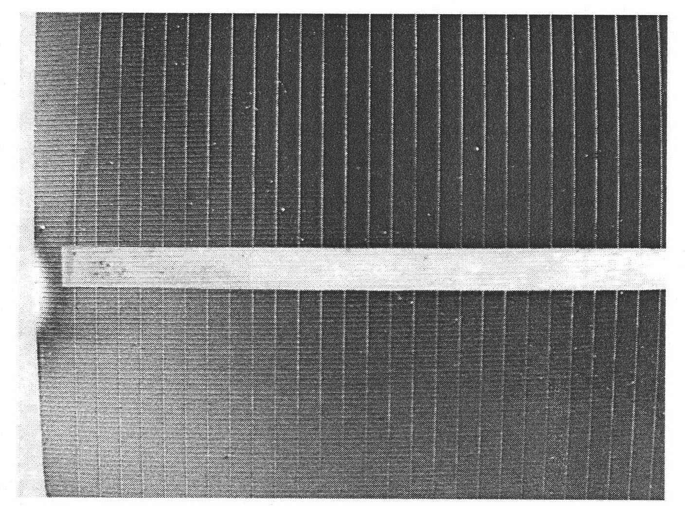
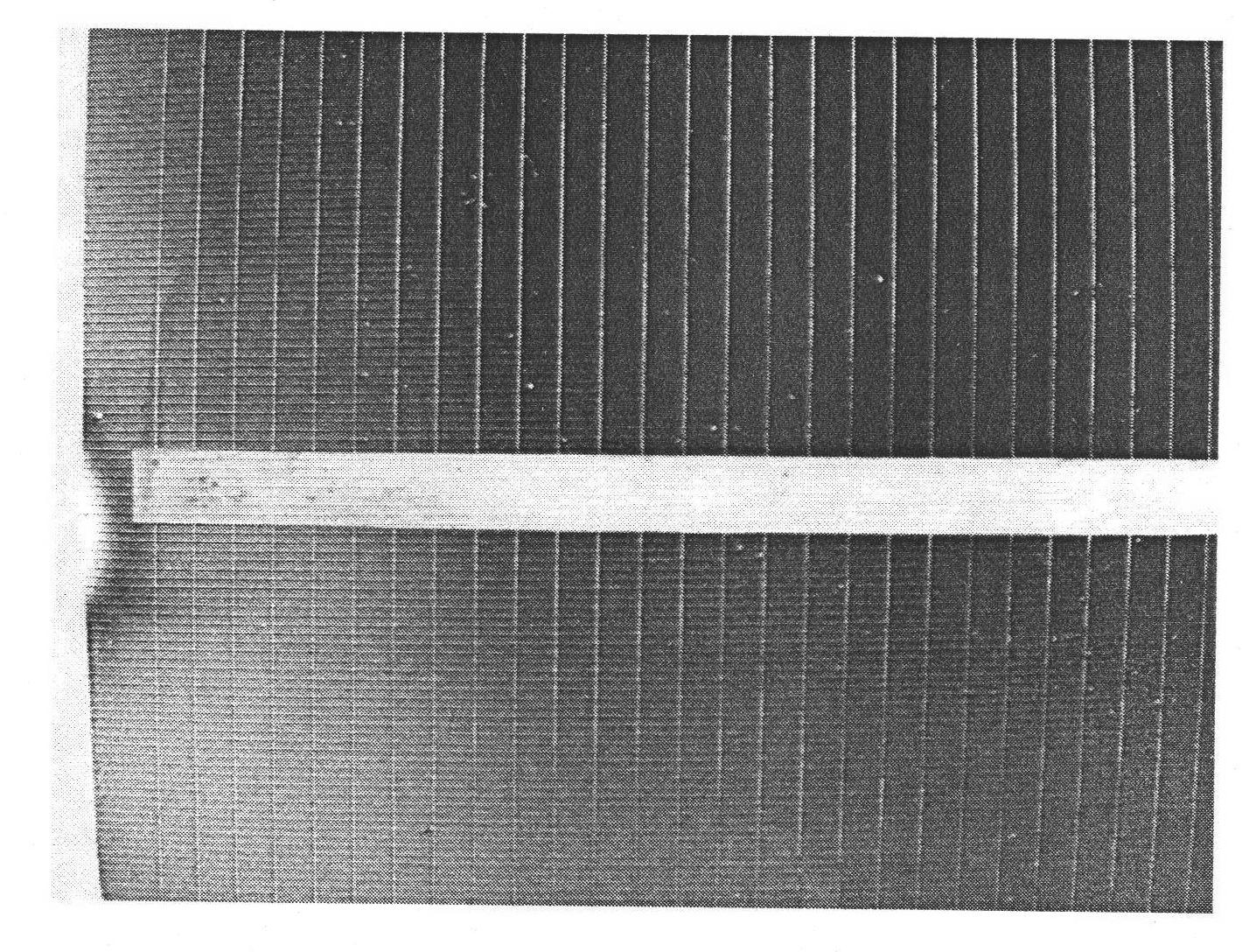
[0036] (2) Laser groove: On the surface of the silicon semiconductor coated with a protective film, an array groove with a depth of 10 μm and a width of 10 μm is carved by laser;

[0037] (3) Surface activation treatment: After the silicon semiconductor with the array groove carved is cleaned by fatty alcohol polyoxyethylene ether sodium sulfate with a mass percentage concentration of 5%, the groove is treated in a HF hydrochloric acid solution with a mass percentage concentration of 5%. Activation was carried out for 5 minutes to obtain a pretreated silicon semiconductor;

[0038] (4) Electroplating: use a conventional electroplating power supply and a conventional electroplating tank, use the cathode of the power su...

Embodiment 2

[0042] (1) protective film coating: coating a layer of alkyd varnish on the surface of a silicon semiconductor coated with a porous silicon dioxide anti-reflection layer as a protective film; the silicon semiconductor is polysilicon with a p / n junction;

[0043] (2) Laser groove: On the surface of the silicon semiconductor coated with a protective film, an array groove with a depth of 20 μm and a width of 20 μm is carved by laser; short circuit;

[0044] (3) Surface activation treatment: After cleaning the silicon semiconductor with array grooves with a mass percentage concentration of 0.5% sodium dodecylbenzene sulfonate, the grooves are aligned in a 5% mass percentage concentration of sodium hydroxide solution. The tank is activated for 0.5min to obtain a pretreated silicon semiconductor;

[0045] (4) Electroplating: use a conventional electroplating power supply and a conventional electroplating tank, use the cathode of the power supply to connect the pretreated semiconduc...

Embodiment 3

[0049] (1) Protective film coating: a layer of nitro varnish is coated on the surface of a silicon semiconductor coated with a titanium dioxide anti-reflection layer as a protective film; the silicon semiconductor is a single crystal silicon with a p / n junction;

[0050] (2) Laser grooving: On the surface of the silicon semiconductor coated with a protective film, an array groove with a depth of 30 μm and a width of 30 μm is carved by laser;

[0051] (3) Surface activation treatment: After the silicon semiconductor with the array grooves is cleaned by sodium dodecyl sulfate with a mass percentage concentration of 2%, the NH 4 HF 2 Activate the groove for 10 minutes in a hydrochloric acid solution to obtain a pretreated silicon semiconductor;

[0052] (4) Electroplating: use a conventional electroplating power supply and a conventional electroplating tank, use the cathode of the power supply to connect the pretreated semiconductor crystal silicon, and connect the anode of the ...


PUM


Abstract

The invention discloses a manufacturing method of a grid array electrode of a crystalline silicon solar cell. The method comprises the following steps: (1) protective film coating; (2) laser grooving; (3) surface activation processing; (4) electroplating: adopting a conventional electroplating power source and a conventional electroplating bath, connecting the cathode of the power source to a pre-treated silicon semiconductor, and connecting the anode of the power source to a conduction metal; and turning on the power source, and electroplating at the current density of 0.5-10 A / dm<2>; and (5) protective film removing. Using the method, the production efficiency is obviously raised to realize the preparation of the electrode array in a shorter time, the prepared electrode is uniform and bright, and meanwhile, the bath solution is easy to be maintained; and compared with the commonly-used chemical plating, screen printing and the like, the remedies used in the method for preparing the electrode by direct electroplating are cheaper, and are easy to be obtained. The invention is beneficial to emission reduction, consumption lowing and production cost decrease; and the method has the advantages of simple operation, high bonding force between the electrode wire and the matrix, uniformity and low void ratio.

Description

technical field [0001] The invention belongs to the technical field of surface treatment of crystalline silicon materials, and in particular relates to a method for manufacturing grid-like array electrodes with p / n crystalline silicon solar cells. Background technique [0002] With the increasing tension of global energy sources, solar energy has unique advantages such as no pollution, no mechanical rotating parts, easy maintenance, unattended operation, short construction period, random scale, easy combination with buildings, and large market space. The advantages are widely valued by countries all over the world, and many large companies in the world have invested in the research and development and production of solar cells. [0003] In the past ten years, the application cost of silicon solar cells has been greatly reduced by reforming manufacturing methods and improving product performance. However, it is necessary to further reduce the manufacturing cost and improve t...

Claims


Application Information

Patent Timeline
IPC IPC(8): H01L31/18H01L31/0224
CPCY02P70/50
Inventor 莫烨强黄启明吴飞黄美玲李伟善
Owner SOUTH CHINA NORMAL UNIVERSITY
Why Eureka
Try Eureka