Double-layer structure deep-ultraviolet transparent conductive film and preparation method thereof

A transparent conductive film, double-layer structure technology, applied in semiconductor/solid-state device manufacturing, coatings, circuits, etc., can solve the problems of high sheet resistance, expensive equipment, and difficulty in forming large-area films.

Inactive Publication Date: 2010-09-22
LUDONG UNIVERSITY
View PDF1 Cites 10 Cited by
  • Summary
  • Abstract
  • Description
  • Claims
  • Application Information

AI Technical Summary

Problems solved by technology

The equipment of pulsed laser deposition method is expensive, and it is difficult to form a large area film; Sn-doped β-Ga prepared by pulsed laser deposition method 2 o 3 The sheet resistance is too high, and there is still a long way to go before practical commercial applications

Method used


Image

  • Double-layer structure deep-ultraviolet transparent conductive film and preparation method thereof
  • Double-layer structure deep-ultraviolet transparent conductive film and preparation method thereof
  • Double-layer structure deep-ultraviolet transparent conductive film and preparation method thereof

Examples


Embodiment 1

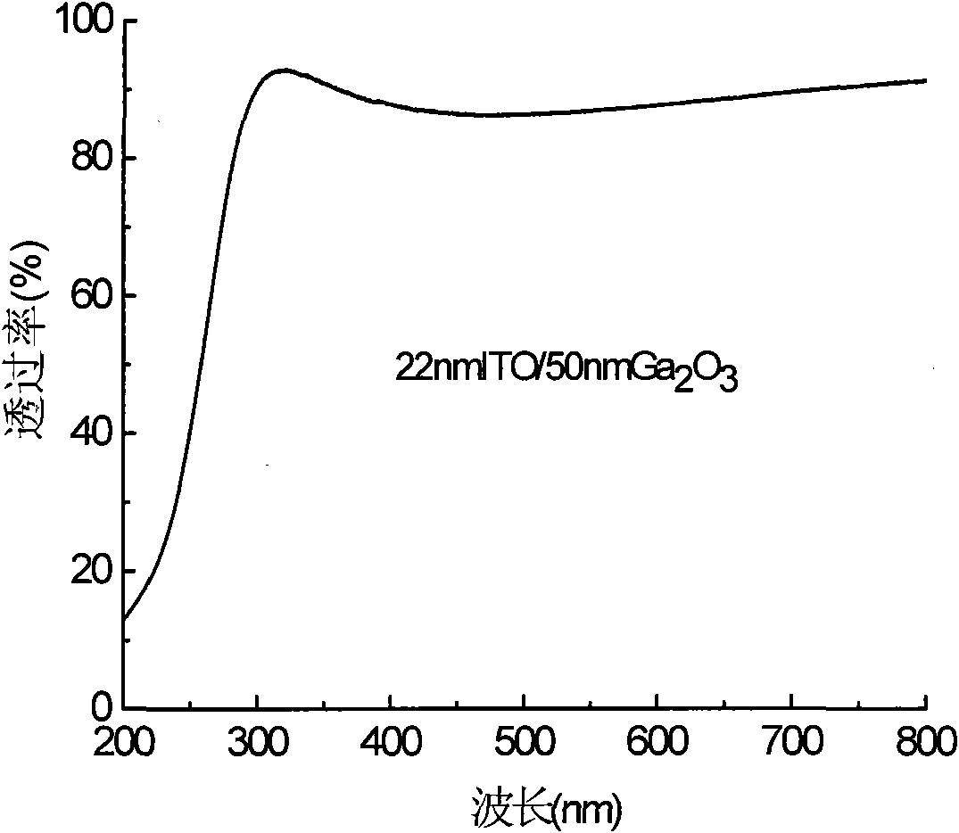
[0019] Example 1: 22nmITO / 50nmGa 2 O 3

[0020] The substrate is made of JGS1 far-ultraviolet optical quartz glass, the substrate is ultrasonically cleaned with acetone, alcohol and deionized water, and dried with a nitrogen gun. Ga with a purity of 99.99wt% 2 O 3 The ceramic target is installed in a radio frequency cathode target tank in the magnetron sputtering chamber, and the SnO 2 / (In 2 O 3 +SnO 2 ) An ITO target material with a ratio of 10 wt% is installed in a DC cathode target tank in the magnetron sputtering chamber. Put the cleaned JGS1 far ultraviolet optical quartz glass into the substrate holder, and insert the substrate holder into the substrate tray in the sputtering chamber. Use mechanical pumps and molecular pumps to vacuum the sputtering chamber, so that the vacuum degree of the sputtering chamber is less than 6.0×10 -4 Pa. Set a temperature controller to adjust the heating current to heat the substrate to stabilize the substrate temperature at 250°C. Adjust ...

Embodiment 2

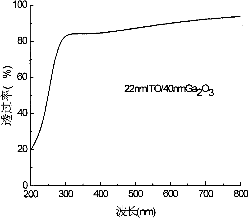
[0021] Example 2: 22nmITO / 40nmGa 2 O 3

[0022] The preparation process is the same as in Example 1, except that the radio frequency sputtering deposition of Ga 2 O 3 The layer thickness is 40nm. Using the above process to finally form a double-layer structure 22nmITO / 40nmGa 2 O 3 Deep ultraviolet transparent conductive film. The prepared double-layer structure 22nmITO / 40nmGa 2 O 3 The transmittance curve of deep ultraviolet transparent conductive film in the range of 200-800nm ​​is as follows figure 2 Shown. The optical transmittance at 280nm (without substrate) is 75.8%, the optical transmittance at 300nm (without substrate) is 82.6%, and the average transmittance (without substrate) in the 300-800nm ​​spectral range is higher than 86%. The sheet resistance is 334Ω, and the sheet resistivity is 2.07×10 -3 Ω.cm.

Embodiment 3

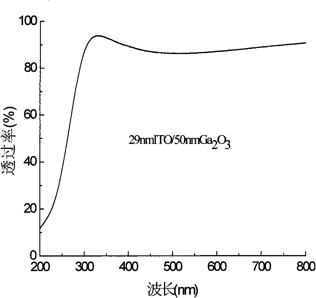
[0023] Example 3: 29nmITO / 50nmGa 2 O 3

[0024] The preparation process is the same as in Example 1, except that the substrate uses JGS2 ultraviolet optical quartz glass, the substrate temperature is 300℃, the sputtering gas argon pressure is 1.0Pa, the RF sputtering power is 60W, the DC sputtering current is 140mA, and the DC sputtering voltage is 360V. , The thickness of the sputter deposited ITO layer is 29nm. Using the above process to finally form a double-layer structure 29nmITO / 50nmGa 2 O 3 Deep ultraviolet transparent conductive film. Prepared 29nmITO / 50nm Ga 2 O 3 The transmittance curve of the double-layer structure deep ultraviolet transparent conductive film in the range of 200-800nm ​​is as follows image 3 Shown. The optical transmittance at 280nm (without substrate) is 70.9%, the optical transmittance at 300nm (without substrate) is 87.5%, and the average transmittance (without substrate) in the 300-800nm ​​spectral range is higher than 88%. The sheet resistance ...


PUM

PropertyMeasurementUnit
thicknessaaaaaaaaaa
thicknessaaaaaaaaaa
thicknessaaaaaaaaaa

Abstract

The invention relates to a tin-doped indium oxide (ITO)/gallium oxide (Ga2O3) double-layer structure deep-ultraviolet transparent conductive film and a preparation method thereof, and belongs to the technical field of electronic materials. The preparation method comprises the following steps: ultraviolet optical quartz glass is used as the substrate, and radio-frequency magnetron sputtering is carried out on the Ga2O3 ceramic target to prepare a Ga2O3 layer the thickness of which is 30-60 nm; and direct-current magnetron sputtering is carried out on an ITO target to prepare an ITO layer the thickness of which is 15-29 nm. The pressure intensity of argon gas for sputtering is 0.2-2 Pa, the power for radio-frequency sputtering is 50-100 W, the substrate temperature is 200-300 DEG C, the current for direct-current sputtering is 80-150 mA, and the voltage for direct-current sputtering is 200-400 V. The prepared film has the advantages of low resistivity, high transmittivity within the range of visible light, ultraviolet light and deep-ultraviolet light, and other favorable photoelectric properties. The film otained by the method of the invention has wide application prospects in the fields of ultraviolet photoelectric devices and the like.

Description

(1) Technical field: [0001] The invention relates to a double-layer structure deep ultraviolet transparent conductive film and a preparation method thereof, and belongs to the technical field of electronic materials. (2) Background technology: [0002] Deep ultraviolet light-emitting diodes are widely used in high-density optical recording, excitation light sources for biological and chemical sensors, safety communications, space technology, medical treatment, and high-speed decomposition and treatment of pollutants. So far, ultraviolet lasers and gas lamps with gas and solid media such as excimer lasers and various frequency doubled lasers have been the mainstream of deep ultraviolet light sources, which have the disadvantages of large volume, short life, and high price, making it difficult to practically apply. Organic electroluminescent devices (OLEDs) have received widespread attention due to their high efficiency, high brightness, wide viewing angle, low power consumption, s...

Claims


Application Information

Patent Timeline
Patent Type & Authority Applications(China)
IPC IPC(8): H01L51/52H01L51/56C23C14/35C23C14/08
Inventor 闫金良李厅张易军赵银女
Owner LUDONG UNIVERSITY
Why Eureka
Try Eureka