Array substrate, manufacturing method thereof, and wide viewing angle liquid crystal display

A technology of array substrates and substrate substrates, which is applied in semiconductor/solid-state device manufacturing, instruments, electric solid-state devices, etc., can solve problems such as increased equipment investment, and achieve the effects of small equipment investment, reduced costs, and increased film thickness

Active Publication Date: 2011-12-28
BOE TECH GRP CO LTD
View PDF0 Cites 0 Cited by
  • Summary
  • Abstract
  • Description
  • Claims
  • Application Information

AI Technical Summary

Problems solved by technology

However, the increase in the thickness of the passivation layer requires an increase in the number of plasma-enhanced chemical vapor deposition (PlasmaEnhanced Chemical Vapor Deposition; hereinafter referred to as: PECVD) equipment and dry etching equipment to ensure the process matching of the production line, resulting in a substantial increase in equipment investment

Method used


Image

  • Array substrate, manufacturing method thereof, and wide viewing angle liquid crystal display
  • Array substrate, manufacturing method thereof, and wide viewing angle liquid crystal display
  • Array substrate, manufacturing method thereof, and wide viewing angle liquid crystal display

Examples


no. 1 example

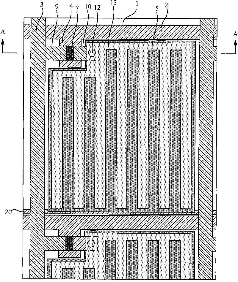
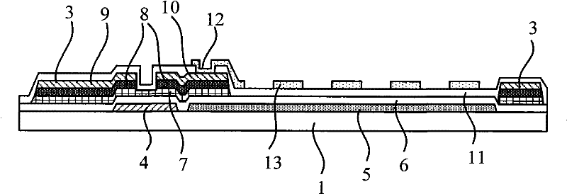
[0041] image 3 It is a schematic cross-sectional structure diagram of the array substrate provided by the first embodiment of the present invention, and its partial top view structure schematic diagram can be found in figure 1 As shown (the gate insulating layer, passivation layer and organic transparent insulating layer are not shown in the plan view herein). The array substrate is specifically an array substrate in an FFS mode liquid crystal display, such as image 3As shown, its specific structure includes: a base substrate 1, usually made of glass; a plurality of data lines 3 and gate lines 2 crossing each other are formed on the base substrate 1, and the data lines 3 and gate lines 2 define a A plurality of pixel areas arranged in matrix form; each pixel area includes common electrode lines 20, common electrodes 5, TFT switches, passivation layers 11 and pixel electrodes 13, and each pixel area is covered with a whole block of common electrodes 5. Corresponding to the ...

no. 2 example

[0055] Figure 4 It is a flow chart of the manufacturing method of the array substrate provided by the second embodiment of the present invention, and the method specifically includes the following steps:

[0056] Step 100, using a patterning process on the base substrate to form patterns of common electrodes, common electrode lines, and TFT switches;

[0057] Step 200, a passivation layer may be deposited on the above-mentioned base substrate by PECVD method;

[0058] Step 300, forming an organic transparent insulating layer on the passivation layer, and using a patterning process to etch on the organic transparent insulating layer to form organic layer via holes, and simultaneously etch the passivation layer to form passivation layer via holes, the organic layer The via hole completely overlaps the passivation layer via hole;

[0059] Step 400, deposit a transparent conductive film layer on the organic transparent insulating layer, and use a patterning process to etch to f...

no. 3 example

[0062] Figure 5 It is a flow chart of the manufacturing method of the array substrate provided by the third embodiment of the present invention, and the method specifically includes the following steps:

[0063] Step 100, using a patterning process on the base substrate 1 to form the patterns of the common electrode 5, the common electrode line 20 and the thin film transistor switch;

[0064] A specific implementation of step 100 is as follows:

[0065] Step 101a, deposit a transparent conductive film layer on the base substrate 1, and use a patterning process to etch to form a pattern of the common electrode 5, such as Figure 6 and Figure 7 shown;

[0066] Step 102a, deposit a gate metal layer on the above-mentioned substrate 1, and use a patterning process to etch to form the pattern of the common electrode line 20, the gate line 2 and the gate electrode 4, as Figure 8 and Figure 9 shown;

[0067] Step 103a, depositing a gate insulating layer 6 on the above-mentio...


PUM

PropertyMeasurementUnit
thicknessaaaaaaaaaa
thicknessaaaaaaaaaa

Abstract

The invention relates to an array substrate, a manufacturing method thereof and a liquid crystal display with a wide viewing angle. The array substrate includes a base substrate and a plurality of pixel regions, and also includes an organic transparent insulating layer formed between the passivation layer and the pixel electrodes. The manufacturing method includes: forming a common electrode, a common electrode line, and a pattern of a thin film transistor switch on a base substrate; depositing a passivation layer; forming an organic transparent insulating layer on the passivation layer, and forming an organic layer via hole and a passivation layer A via hole: a pattern of the pixel electrode is formed on the organic transparent insulating layer, the pattern of the pixel electrode has a plurality of gaps, and the pixel electrode is connected to the thin film transistor switch through the organic layer via hole and the passivation layer via hole. The liquid crystal display of the present invention includes the array substrate of the present invention. The invention adopts the technical means of adding an organic transparent insulating layer between the pixel electrode and the passivation layer, increases the thickness of the film layer between the pixel electrode and the common electrode, can effectively reduce the storage capacitance and reduce afterimages.

Description

technical field [0001] The invention relates to liquid crystal display technology, in particular to an array substrate, a manufacturing method thereof, and a wide viewing angle liquid crystal display. Background technique [0002] The market of liquid crystal display is growing rapidly, and the application fields are continuously expanding, especially the application of large-size liquid crystal TV, which requires the liquid crystal display to have a wide range of viewing angles. The main part of the liquid crystal display, the liquid crystal panel, includes an array substrate and a color filter substrate arranged in opposite cells, and a liquid crystal layer is arranged between them. The liquid crystal molecules are deflected under the action of the voltage, and the degree of deflection of the liquid crystal molecules can be controlled by controlling the magnitude of the voltage, so as to achieve the purpose of adjusting the transmittance, that is, adjusting the gray scale ...

Claims


Application Information

Patent Timeline
Patent Type & Authority Patents(China)
IPC IPC(8): H01L27/12H01L23/522H01L21/84H01L21/768G02F1/1362G02F1/1333
Inventor 邵喜斌齐悦张丽蕾金哲雄
Owner BOE TECH GRP CO LTD
Why Eureka
Try Eureka