Preparation method of high-temperature and high-power field effect transistor

A field-effect transistor and high-power technology, which is applied in the field of high-temperature, high-power metal-oxide-semiconductor field-effect transistor preparation, can solve the problems of many defects, difficult speed improvement, poor uniformity, etc., and achieve good temperature stability sex, performance-improving effects

Inactive Publication Date: 2010-10-13
SHANGHAI UNIV
View PDF2 Cites 8 Cited by
  • Summary
  • Abstract
  • Description
  • Claims
  • Application Information

AI Technical Summary

Problems solved by technology

[0005] Due to the extremely difficult preparation of single crystal diamond films, the doped diamond-based FETs currently being developed in the world all use polycrystalline diamond films, while polycrystalline diamond films have chaotic grain boundaries, many defects, rough surfaces,

Method used


Image

  • Preparation method of high-temperature and high-power field effect transistor
  • Preparation method of high-temperature and high-power field effect transistor
  • Preparation method of high-temperature and high-power field effect transistor

Examples


Embodiment

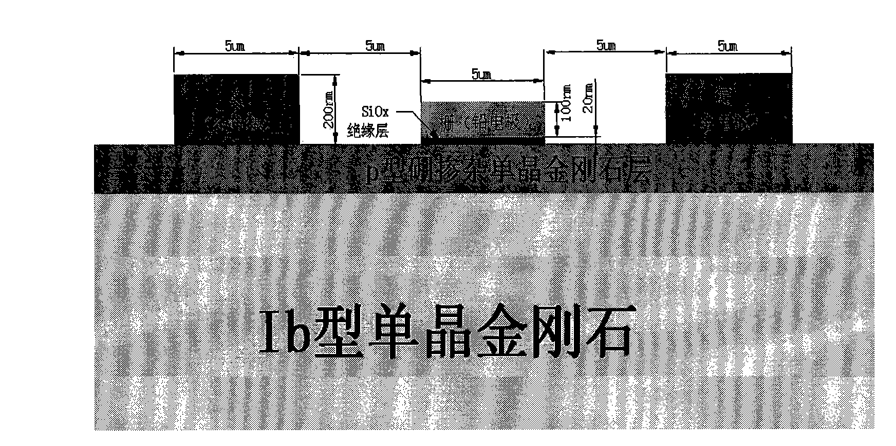
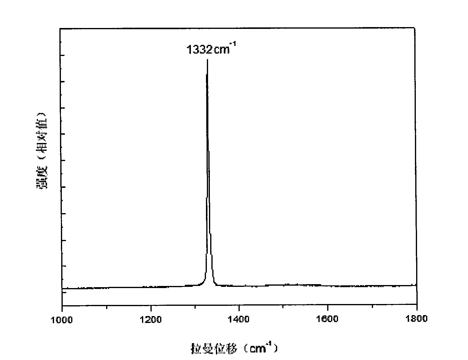
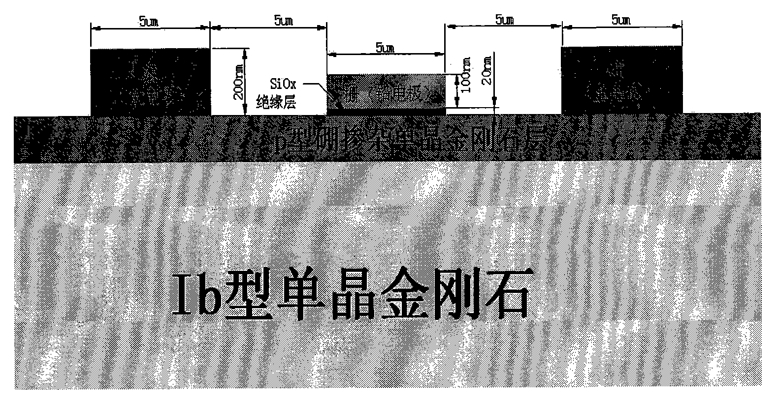
[0024] In this embodiment, the preparation process and steps of a semiconductor field effect transistor based on a p-type doped single crystal diamond film are as follows:

[0025] (1) Preparation of p-type boron-doped single-crystal diamond thin film: use purchased 2×2mm 2 I b type single crystal diamond as the deposition substrate. Ultrasonic cleaning in acetone solution for 10 minutes, dried and placed in a microwave plasma chemical vapor deposition (MPCVD) device.

[0026] First use a vacuum pump to evacuate the MPCVD reaction chamber to 5Pa, and then use a molecular pump to evacuate the reaction chamber to 5×10 -3 Pa, feed the mixed reaction gas of methane, hydrogen and diborane, adjust the flow of methane, hydrogen and diborane to be 1 standard ml / min, 120 standard ml / min and 2 standard ml / min respectively; the air pressure in the reaction chamber The setting is 0.2kPa, the substrate temperature is controlled at 690°C, the microwave power is set at 2350W, and the film...


PUM

PropertyMeasurementUnit
Thicknessaaaaaaaaaa

Abstract

The invention relates to a preparation method of a high-temperature and high-power metal-oxide-semiconductor field effect transistor (MOSFET) based on a p-shaped boron-doped single-crystal diamond film, which belongs to the technical field of production processes of inorganic nonmetal metal devices. The preparation method is mainly characterized by comprising the following steps: producing a source electrode, a drain electrode and a grid electrode on the p-shaped boron-doped single-crystal diamond film; using gold electrodes as the source electrode and the drain electrode and using a lead electrode as the grid electrode; and adopting SiOx as an insulating layer between the grid electrode and a p-shaped diamond film. The p-shaped boron-doped single-crystal diamond film is deposited by adopting a microwave plasma chemical vapor deposition method (MPCVD) and a semiconductor field effect transistor device is prepared on the basis. The stable work temperature of the device can reach 690DEG C.

Description

technical field [0001] The invention relates to a method for preparing a high-temperature, high-power metal-oxide-semiconductor field-effect transistor (MOSFET) based on a p-type doped single-crystal diamond film, and belongs to the technical field of inorganic metal material device manufacturing technology. Background technique [0002] A field effect transistor (field effect transistor, FET) is a three-terminal active device, which controls the magnitude of the current at the other two ends (source, drain) through the power supply of the third terminal (gate). Among various FETs, oxide-semiconductor field effect transistor (MOSFET) is the most important and widely used device in VLSI such as microprocessor and semiconductor memory. [0003] At present, FETs generally use Si and GaAs materials. However, due to the limitations of their own physical properties, these materials have a relatively low operating temperature (theoretical limit operating temperature is less than 1...

Claims


Application Information

Patent Timeline
IPC IPC(8): H01L21/335H01L21/365H01L21/28
Inventor 王林军张凤娟黄健唐可曾庆锴夏辅元张继军闵嘉华
Owner SHANGHAI UNIV
Why Eureka
Try Eureka