Quantum cascade laser with photonic quasi-crystal waveguide and manufacture method thereof

A quasi-photonic crystal and quantum cascade technology, which is applied in semiconductor lasers, lasers, phonon exciters, etc., can solve problems affecting the application of quantum cascade lasers

Inactive Publication Date: 2010-10-13
INST OF SEMICONDUCTORS - CHINESE ACAD OF SCI
View PDF0 Cites 26 Cited by
  • Summary
  • Abstract
  • Description
  • Claims
  • Application Information

AI Technical Summary

Problems solved by technology

[0003] In the field of practical use, in order to effectively couple the laser with the optical fiber, it is generally required that the laser has a small far-field divergence angle of the outgoing beam, but because the active region of the quantum cascade laser is very thin, only 2-3μm, and the lasing wavelength It is also in the mid-infrared band, so the far-field divergence angle is generally greater than 50°, which greatly affects the application of quantum cascade lasers in communications

Method used


Image

  • Quantum cascade laser with photonic quasi-crystal waveguide and manufacture method thereof
  • Quantum cascade laser with photonic quasi-crystal waveguide and manufacture method thereof
  • Quantum cascade laser with photonic quasi-crystal waveguide and manufacture method thereof

Examples


Embodiment Construction

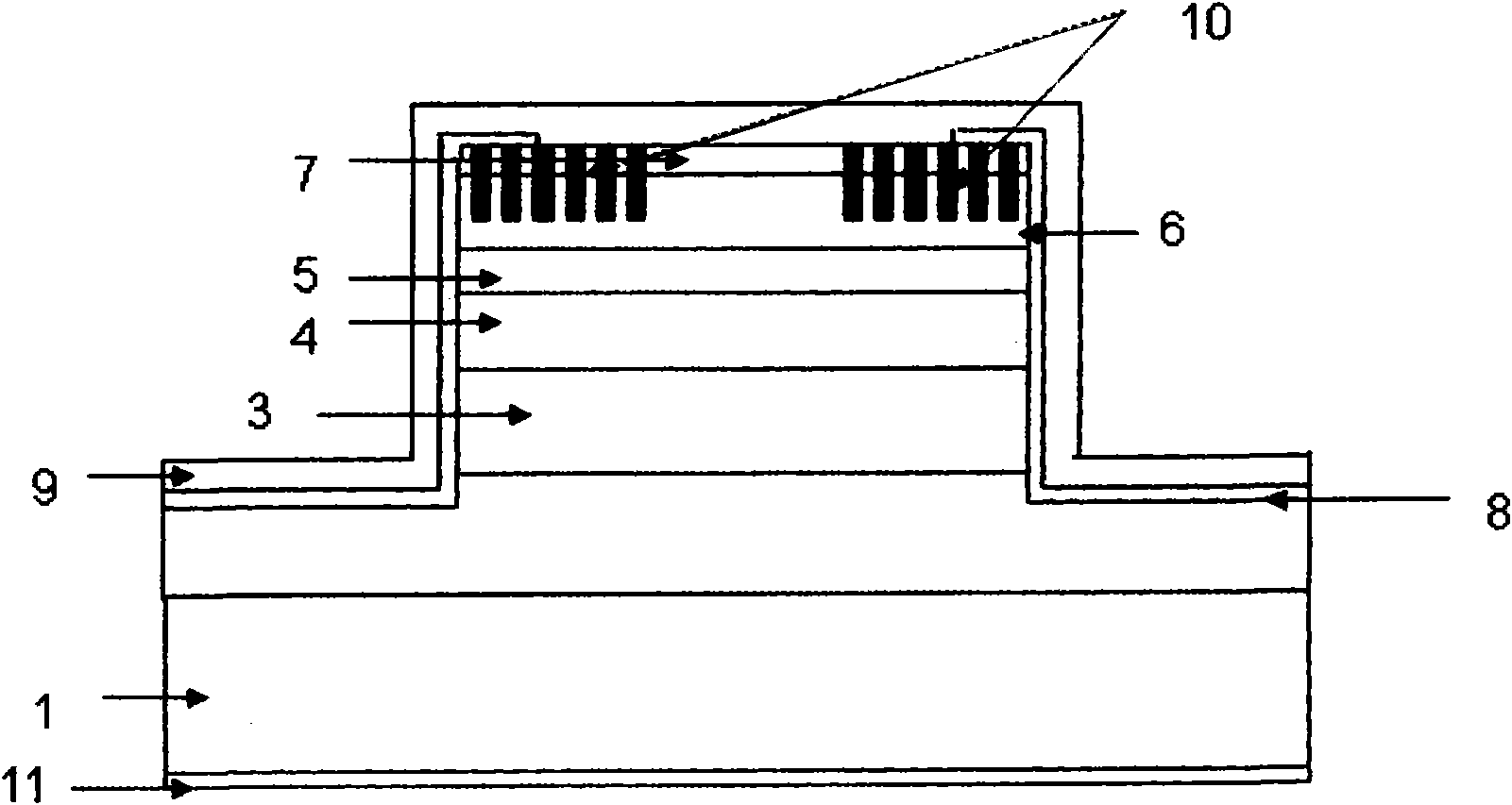
[0043] In the following, the present invention will be further described by taking the InP / InGaAs / InAlAs material system and quantum cascade laser with weakly disordered quasi-photonic crystal waveguide as an example, but this does not constitute a limitation to the present invention.

[0044] The invention provides a quantum cascade laser structure with a weakly disordered quasi-photonic crystal waveguide structure, including an n-type doped InP substrate, an InGaAs lower waveguide layer, a 35-level periodic quantum cascade active region structure, and an InGaAs upper Waveguide layer, InP upper cladding layer, InP upper cladding layer, highly doped InP ohmic contact layer, quasi-photonic crystal waveguide, double-groove-ridge structure. See the specific structure figure 1 Shown is a schematic cross-sectional structure diagram of the present invention, including:

[0045] A substrate 1; the substrate is an n-type doped InP substrate with a doping concentration of 1-3×10 17 c...


PUM


Abstract

The invention relates to a quantum cascade laser with a photonic quasi crystal waveguide, comprising a substrate, a lower waveguide layer, a quantum cascade active area structure, an upper waveguide layer, an upper cladding, an upper covering layer, a high-doping ohmic contact layer, a photonic quasi crystal structure array, an electric insulation layer, a front electrode and a back electrode, wherein the lower waveguide layer is grown on the substrate, the middle of the lower waveguide layer is provided with a boss, and a ridge-shaped double-groove table-board structure is formed at both sides of the boss; the quantum cascade active area structure is grown on the boss of the lower waveguide layer; the upper waveguide layer is grown on the quantum cascade active area structure; the upper cladding is grown on the upper waveguide layer; the upper covering layer is grown on the upper cladding; the high-doping ohmic contact layer is grown on the upper covering layer; the photonic quasi crystal structure array is manufactured at both sides of the upper covering layer and the high-doping ohmic contact layer, the middle width is 2-10 mu m, and the widths of the photonic quasi crystal structure array at both sides are the same and are respectively 5-24 mu m; the electric insulation layer is deposited on the ohmic contact layer and covers the upper surface and the side wall of the whole ridge-shaped table-board, and the central part of the ridge-shaped table-board, covered with the insulation layer, is reserved with an electric injection window; the front electrode is manufactured on the insulation layer; and the back electrode is grown on the back of the substrate.

Description

technical field [0001] The invention relates to the field of semiconductor optoelectronics, in particular to a quantum cascade laser with a weakly disordered quasi-photonic crystal waveguide structure and a manufacturing method thereof. Background technique [0002] The mid-to-far infrared band with a wavelength of 3-14 μm is a very important large device window. Lasers and detectors working in this band have a wide range of applications in military, medical, environmental protection, gas detection, chemical spectroscopy, free space communication, etc. prospect. In 1994, Bell Laboratories successfully produced the first quantum cascade laser through molecular beam epitaxy technology. Unlike conventional semiconductor lasers, the lasing wavelength of this laser device has nothing to do with the forbidden band width of the quantum cascade active region material. It is mainly determined by the quantum cascade active region structure, that is, the thickness of the quantum well,...

Claims


Application Information

Patent Timeline
Patent Type & Authority Applications(China)
IPC IPC(8): H01S5/34H01S5/227H01S5/06
Inventor 尹雯陆全勇张伟刘峰奇张全德刘万峰江宇超李路刘俊岐王利军王占国
Owner INST OF SEMICONDUCTORS - CHINESE ACAD OF SCI
Why Eureka
Try Eureka