

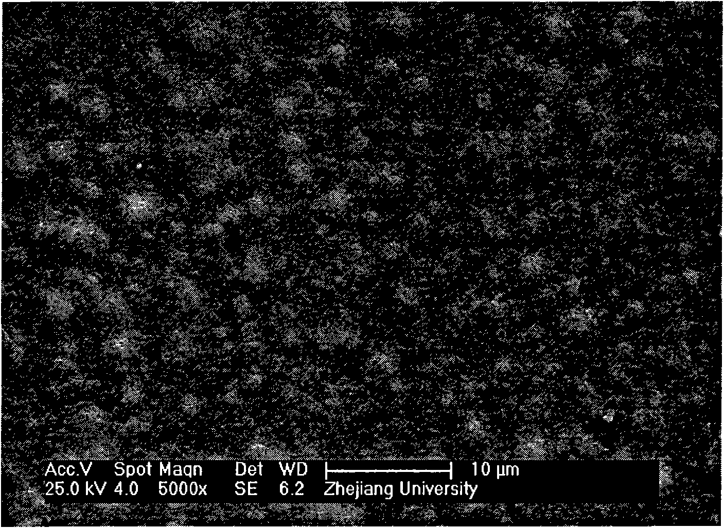
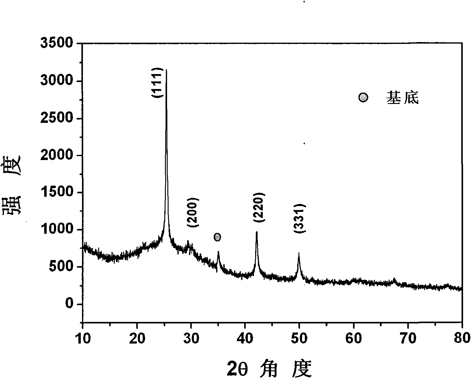
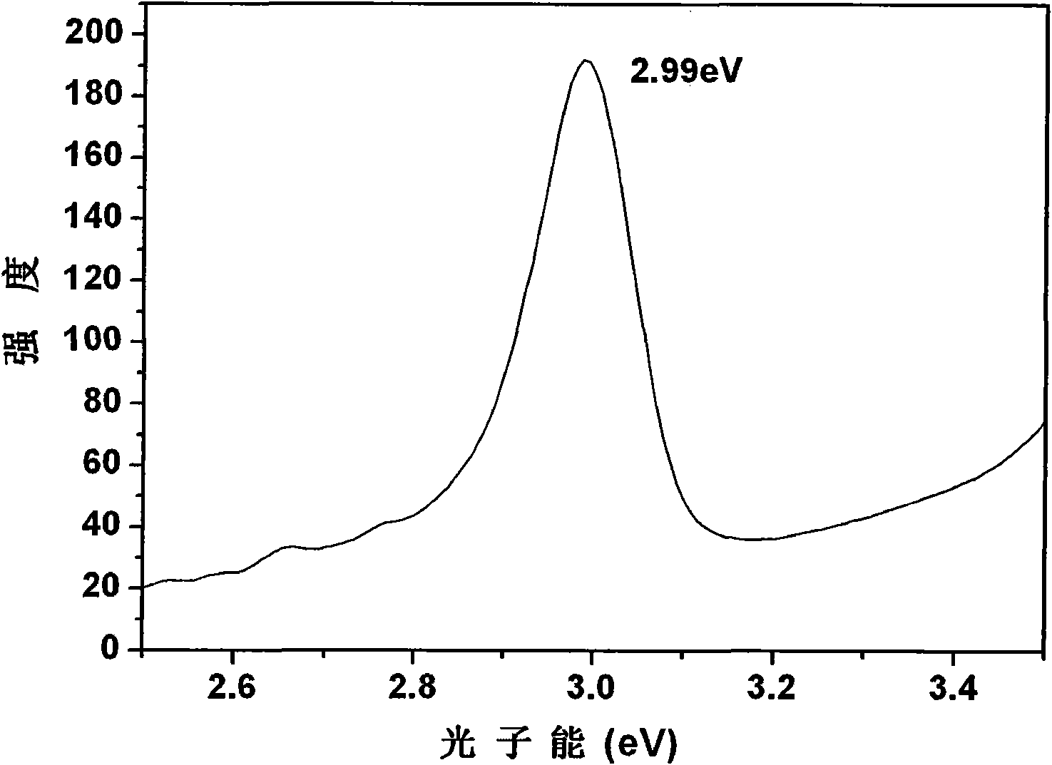
Electrochemical preparation method of uniform and compact cuprous iodide semiconductor film
A cuprous iodide and semiconductor technology, which is applied in the field of electrochemical preparation of uniform and dense cuprous iodide semiconductor thin films, can solve problems such as the inability to obtain good thin film materials, and achieves good compactness, mild preparation conditions and low cost. Effect
- Summary
- Abstract
- Description
- Claims
- Application Information
AI Technical Summary
Problems solved by technology
Method used
Image

Examples
Embodiment 1
[0015] 1) Rinse the ITO conductive glass or silicon chip with acetone twice, then clean the ITO conductive glass or silicon chip in an ultrasonic cleaner with deionized water, and then put the ITO conductive glass or silicon chip in 10% nitric acid solution Activated, and finally rinsed repeatedly with deionized water;
[0016] 2) 0.002mol / L of Cu(NO 3 ) 2 , KI of 0.002mol / L, 3.4×10 -6 mol / L of K30 polyvinylpyrrolidone mixed with 2mol / L of HNO 3 or 0.1mol / L NaOH solution to adjust the pH value to 5 to obtain an electrolyte;
[0017] 3) ITO conductive glass or silicon wafer is used as working electrode, platinum sheet electrode is used as counter electrode, and saturated calomel electrode is put into electrolyte together as reference electrode for electrodeposition to obtain dense cuprous iodide semiconductor film. The electrodeposition voltage of the mercury electrode was 0.1 V, the electrodeposition time was 30 minutes, and the electrodeposition temperature was 25° C.
...
Embodiment 2
[0021] 1) Rinse the ITO conductive glass or silicon chip with acetone twice, then clean the ITO conductive glass or silicon chip in an ultrasonic cleaner with deionized water, and then put the ITO conductive glass or silicon chip in 10% nitric acid solution Activated, and finally rinsed repeatedly with deionized water;
[0022] 2) 0.02mol / L of Cu(NO 3 ) 2 , KI of 0.02mol / L, 3.4×10 -5 mol / L of K30 polyvinylpyrrolidone mixed with 2mol / L of HNO 3 or 0.1mol / L NaOH solution to adjust the pH value to 4 to obtain the electrolyte;
[0023] 3) ITO conductive glass or silicon wafer is used as working electrode, platinum sheet electrode is used as counter electrode, and saturated calomel electrode is put into electrolyte together as reference electrode for electrodeposition to obtain dense cuprous iodide semiconductor film. The electrodeposition voltage of the mercury electrode was -0.1V, the electrodeposition time was 20 minutes, and the electrodeposition temperature was 45°C.
[0...
Embodiment 3
[0027] 1) Rinse the ITO conductive glass or silicon wafer with acetone for 3 times, then clean the ITO conductive glass or silicon wafer in an ultrasonic cleaner with deionized water, and then place the ITO conductive glass or silicon wafer in 10% nitric acid solution Activated, and finally rinsed repeatedly with deionized water;
[0028] 2) 0.2mol / L of Cu(NO 3 ) 2 , KI of 0.2mol / L, 3.4×10 -4 mol / L of K30 polyvinylpyrrolidone mixed with 2mol / L of HNO 3 Or 0.1mol / L NaOH solution to adjust the pH value to 2 to obtain the electrolyte;
[0029] 3) ITO conductive glass or silicon chip is used as working electrode, platinum sheet electrode is used as counter electrode, and saturated calomel electrode is put into electrolyte together as reference electrode for electrodeposition, and dense cuprous iodide semiconductor film is obtained. The electrodeposition voltage of the mercury electrode was -0.3V, the electrodeposition time was 15 minutes, and the electrodeposition temperature ...
PUM
 Abstract
Description
Claims
Application Information