Gallium nitride-based inverted light-emitting diode (LED) with two reflecting layers on lateral surfaces and preparation method thereof

A light-emitting diode, gallium nitride-based technology, applied in the direction of electrical components, circuits, semiconductor devices, etc., can solve the problems of limited light reflectivity and low surface resistivity of the reflective layer, achieve excellent reflectivity, and improve the effect of light extraction efficiency

Inactive Publication Date: 2010-10-27
XIAMEN SANAN OPTOELECTRONICS TECH CO LTD
View PDF7 Cites 36 Cited by
  • Summary
  • Abstract
  • Description
  • Claims
  • Application Information

AI Technical Summary

Problems solved by technology

The invention patent application with the Chinese patent application number 200410095820.X discloses a flip-chip light-emitting device and its manufacturing method. The flip-chip light-emitting device includes a substrate, an n-type cladding layer, an active layer, a p-type cladding layer, an ohmic contact layer formed of tin oxide doped with at least one of antimony, fluorine, phosphorus, and arsenic, and a reflective layer formed of a reflective material, by applying a conductive material with low surface resistivity and high carrier concentration The oxide electrode structure improves the current-voltage characteristics and durability; however, this invention uses a single metal layer as the light reflection layer, and the metal film still absorbs part of the light to limit the light output, and the single metal reflection layer is only distributed on the bottom of the chip , there is no distribution on the side, so the light reflectivity of the reflective layer is limited

Method used


Image

  • Gallium nitride-based inverted light-emitting diode (LED) with two reflecting layers on lateral surfaces and preparation method thereof
  • Gallium nitride-based inverted light-emitting diode (LED) with two reflecting layers on lateral surfaces and preparation method thereof
  • Gallium nitride-based inverted light-emitting diode (LED) with two reflecting layers on lateral surfaces and preparation method thereof

Examples


Embodiment Construction

[0036] The present invention will be further described below in conjunction with the accompanying drawings and embodiments.

[0037] A method for preparing a gallium nitride-based flip-chip light-emitting diode with double reflective layers on its side, the steps of which are as follows:

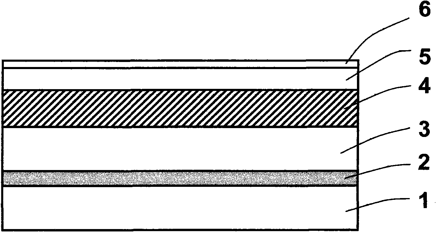
[0038] like figure 1 As shown, a buffer layer 2 and an epitaxial layer are sequentially grown on a sapphire substrate 1, wherein the epitaxial layer includes an N-GaN layer 3, a multi-quantum well layer 4 and a P-GaN layer 5; an ITO layer is formed on the P-GaN layer 5 Transparent conductive layer 6;

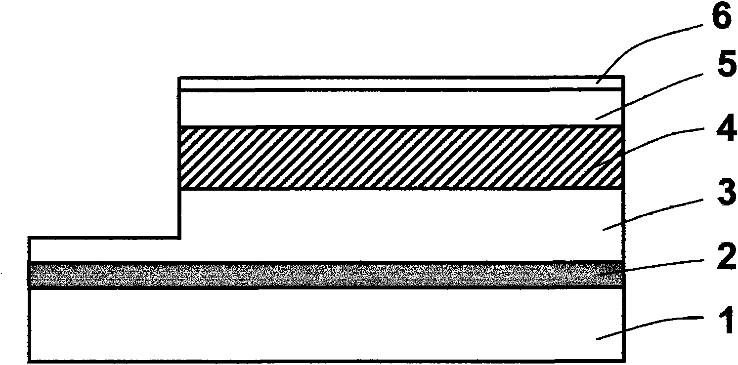
[0039] like figure 2 As shown, through a photomask and etching, the part of the mesa where the ITO transparent conductive layer 6 is located is etched to expose the N-GaN layer 3;

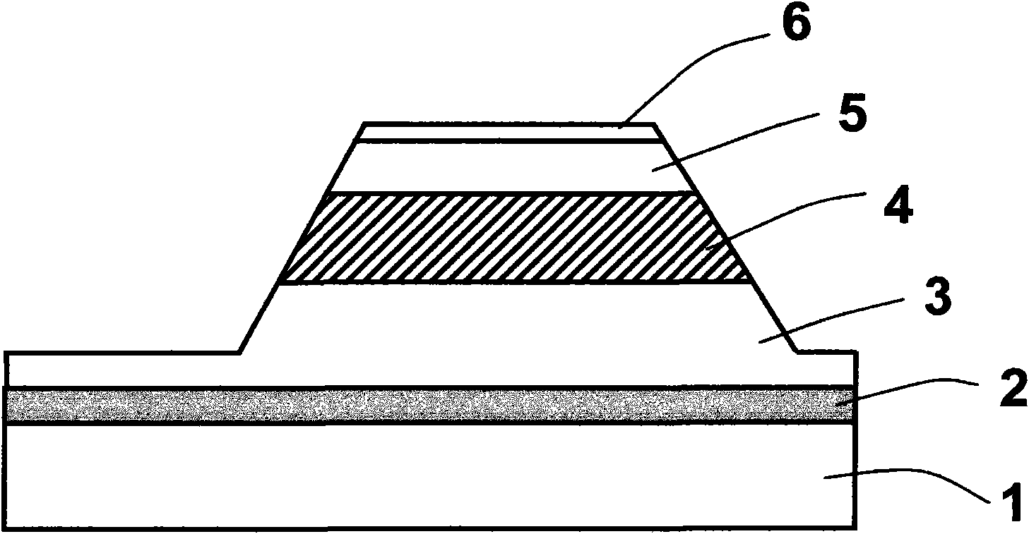
[0040] like image 3 As shown, by cutting, the sides of the epitaxial layer and the ITO transparent conductive layer 6 become inclined;

[0041] like Figure 4 As shown, the distributed Bragg reflection lay...


PUM


Abstract

The invention discloses a dual-reflecting layer gallium nitride-based inverted light-emitting diode (LED) with a distributed Bragg reflecting layer and a metal reflecting layer on lateral surfaces and a preparation method thereof. The preparation method comprises the following steps of: sequentially laminating and forming a buffer layer, a N-GaN layer, a multiple-quantum well layer and a P-GaN layer on a sapphire substrate; forming a transparent conducting layer on the P-GaN layer; covering the distributed Bragg reflecting layer on the lateral surfaces of an epitaxial layer and the transparent conducting layer; forming the metal reflecting layer on the distributed Bragg reflecting layer; forming a P electrode ohmic contact metal layer on an alloy metal reflecting layer; forming a N electrode ohmic contact metal layer on the exposed N-GaN layer; and bonding the P electrode ohmic contact metal layer and the N electrode ohmic contact metal layer with a heat radiating substrate through an alloy metal conducting layer and gold ball bonding points. A dual-reflection structure combining the distributed Bragg reflecting layer and the metal reflecting layer is arranged on the oblique lateral surface of an LED chip, thereby the excellent reflectivity of the reflecting layers is fully performed and the light-emitting efficiency of the LED is improved.

Description

technical field [0001] The invention relates to a gallium nitride-based light-emitting diode, in particular to a gallium nitride-based flip-chip light-emitting diode with double reflective layers on the side and a preparation method thereof. Background technique [0002] As the efficiency of power-type GaN-based LEDs continues to increase, it is unstoppable for GaN-based LED semiconductor lamps to replace existing lighting sources; however, limited by luminous efficiency and production costs, it is still difficult to popularize and apply semiconductor lighting; The methods of luminous efficiency mainly include the use of graphic substrates, transparent substrates, distributed Bragg reflector (Distributed Bragg Reflector, DBR for short) structure, surface microstructure, flip chip, chip bonding, laser lift-off technology, etc. The invention patent application with the Chinese patent application number 200410095820.X discloses a flip-chip light-emitting device and its manufact...

Claims


Application Information

Patent Timeline
Patent Type & Authority Applications(China)
IPC IPC(8): H01L33/46H01L33/40
CPCH01L33/46H01L33/20H01L33/42
Inventor 郑建森林素慧何安和林科闯
Owner XIAMEN SANAN OPTOELECTRONICS TECH CO LTD
Why Eureka
Try Eureka