
Medium/metal/medium nanostructure membrane and preparation method thereof

A nanostructure and dielectric technology, applied in the fields of nanostructure manufacturing, nanotechnology, nanotechnology, etc., can solve the problems of enhancement, metal/dielectric double-layer structure has not seen relevant reports, and achieve long service life and high luminescence enhancement factor. Effect

Inactive Publication Date: 2010-11-17
ZHEJIANG UNIV
View PDF3 Cites 6 Cited by
  • Summary
  • Abstract
  • Description
  • Claims
  • Application Information

AI Technical Summary

Problems solved by technology

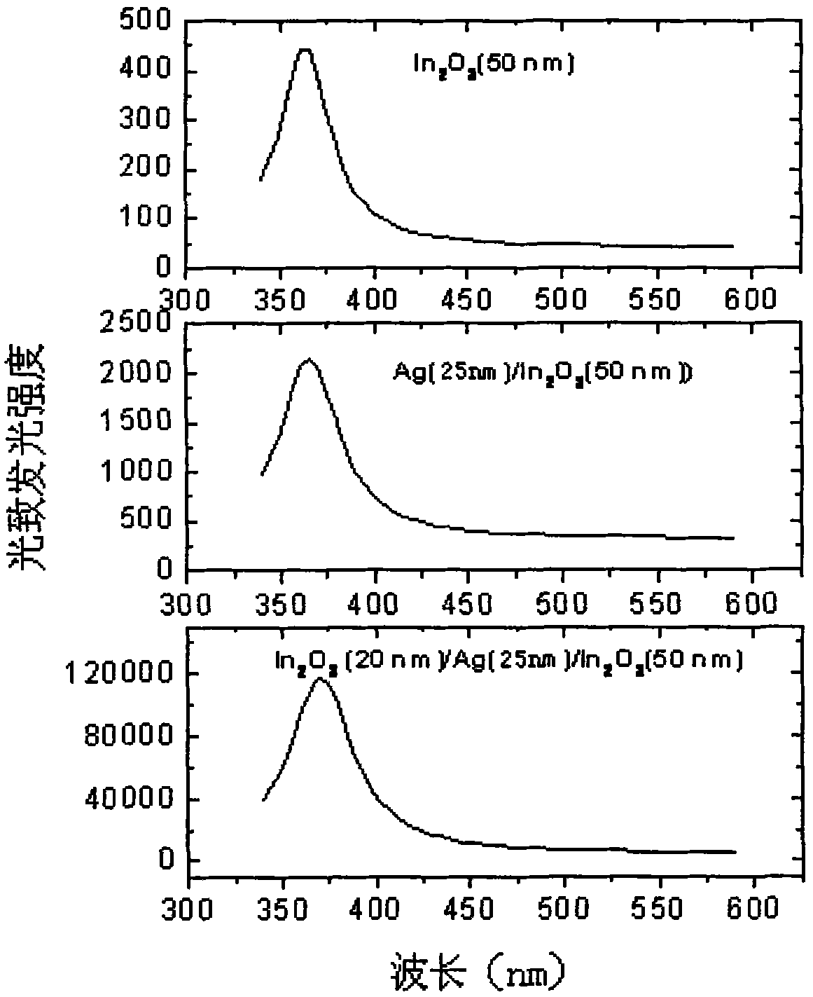
At present, some progress has been made in improving the external quantum efficiency of the metal / dielectric double-layer structure, that is, introducing periodic rough surfaces into the metal layer of the metal / dielectric double-layer structure to enhance the light scattering effect so that the light to the free space The output is enhanced, but there is no relevant report on how to improve the internal quantum efficiency of the metal / dielectric double-layer structure

Method used

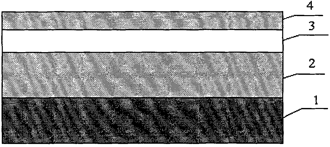
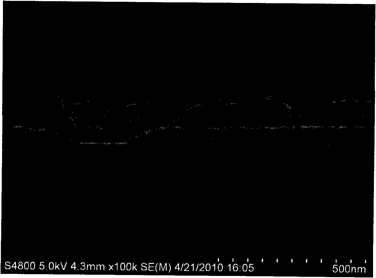

Image

  • Medium/metal/medium nanostructure membrane and preparation method thereof
  • Medium/metal/medium nanostructure membrane and preparation method thereof
  • Medium/metal/medium nanostructure membrane and preparation method thereof

Examples


Embodiment 1

[0040] Preparation of In by electron beam evaporation 2 o 3 (20nm) / Ag(25nm) / In 2 o 3 (50nm) / Si type nanostructure film:

[0041] (1) Select a polished single-crystal silicon wafer as the substrate material, and grow it by the electron beam method: before the growth, fill the two crucibles with In 2 o 3 For the target and Ag target, put the substrate into the sample holder in the growth chamber; use the vacuum unit (oil diffusion pump + mechanical pump) to evacuate the vacuum to make the background vacuum of the growth chamber reach 1×10 -4 Pa; then the growth chamber is filled with Ar gas with a purity of 99.999%, and the air pressure is controlled at 1×10 -2 Pa; aim high-energy electron beam at In 2 o 3 The target begins to grow the first layer of In 2 o 3 Thin film; the substrate temperature is set to room temperature during growth; the growth rate is 3nm / min, and the thickness is controlled at 50nm;

[0042] (2) When the first layer In 2 o 3 After the thickness ...

Embodiment 2

[0050] Preparation of In by electron beam evaporation 2 o 3 (25nm) / Ag(30nm) / In 2 o 3 (70nm) / Si type nanostructure film:

[0051] (1) Select a polished single-crystal silicon wafer as the substrate material, and grow it by the electron beam method: before the growth, fill the two crucibles with In 2 o 3 Target material and Ag target material, put the substrate into the substrate rack; use the vacuum unit (oil diffusion pump + mechanical pump) to evacuate, so that the background vacuum degree of the growth chamber reaches 5×10 -4 Pa; then the growth chamber is filled with Ar gas with a purity of 99.999%, and the air pressure is controlled at 5×10 -2 Between Pa; align high-energy electron beams to In 2 o 3 The target begins to grow the first layer of In 2 o 3 Thin film; the substrate temperature is set to room temperature during growth; the growth rate is 5nm / min, and the thickness is controlled at 70nm;

[0052] (2) When the first layer In 2 o 3 After the thickness o...

Embodiment 3

[0055] Preparation of In by a combination of magnetron sputtering and thermal evaporation 2 o 3 (50nm) / Ag(21nm) / In 2 o 3 (50nm) / Si type nanostructure film:

[0056] (1) Select a polished single crystal silicon wafer as the substrate material, place it in the sample holder in the growth chamber, and use the vacuum unit (molecular pump + mechanical pump) to vacuum the growth chamber to 1×10 -4 The background vacuum of Pa, then fill the growth chamber with argon, and control the pressure of the growth chamber after filling the argon at 1Pa, and grow the first layer of In with a thickness of 50 nanometers on the substrate surface. 2 o 3For thin films, the substrate temperature is set to room temperature during growth; the growth rate is 6nm / min;

[0057] (2) The first layer of In with a thickness of 50 nanometers will be grown 2 o 3 The sample of the thin film is placed in the sample holder of the thermal evaporation growth chamber, and the second layer of Ag thin film is g...


PUM

PropertyMeasurementUnit
thicknessaaaaaaaaaa
thicknessaaaaaaaaaa
thicknessaaaaaaaaaa

Abstract

The invention discloses a medium / metal / medium nanostructure membrane. The membrane comprises a substrate, a first medium layer, a metal layer and a second medium layer, wherein the first medium layer, the metal layer and the second medium layer are arranged on the substrate in turn; the substrate is a mono-crystalline silicon slice, a mono-crystalline sapphire slice or a quartz glass sheet; the first medium layer and the second medium layer are simultaneously indium oxide layers or zinc oxide layers of which the thicknesses are between 20 and 100 nanometers; the metal layer is a silver layer,a gold layer or an aluminum layer of which the thickness is between 5 and 40 nanometers; and the nanostructure membrane can be prepared by an electron beam evaporation method or a method for combining magnetron sputtering with thermal evaporation. Compared with a metal / medium double-layer structure membrane, the medium / metal / medium nanostructure membrane of the invention has the advantages of high luminescence enhancement factor, long service life and wide development prospect.

Description

technical field [0001] The invention relates to the field of nanostructure thin film preparation, in particular to a medium / metal / dielectric nanostructure thin film and a preparation method thereof. Background technique [0002] Surface plasmons (Surface Plasmons, SPs) refer to electron density waves propagating along the metal surface generated by the interaction between freely vibrating electrons and photons existing on the metal surface; since Ritchie first proposed the concept of surface plasmons (R.H.Ritchie, Plasma losses by fast electrons in thin films, Phys.Rev.106, 874, 1957), surface plasmons have played an important role in basic research and technical applications. At present, surface plasmons have been applied in many fields such as sensors, surface-enhanced spectroscopy, light transmission enhancement, nano-optical waveguides, and new high-brightness nano-light sources. [0003] Introducing surface plasmons is an effective way to improve the luminescence effic...

Claims


Application Information

Patent Timeline
Patent Type & Authority Applications(China)
IPC IPC(8): B82B1/00B82B3/00B32B9/04B32B15/04
Inventor 邱东江
Owner ZHEJIANG UNIV
Learn More