Ten-bit superspeed CMOS digital to analog converter based on MOS current mode logic

A digital-to-analog converter and current-mode logic technology, applied in the field of microelectronics, can solve the problems of sacrificing speed performance, aggravating switching noise, affecting circuit accuracy, etc., to eliminate glitches and traps, improve linearity, and avoid misoperation.

Inactive Publication Date: 2010-12-08
XIDIAN UNIV
View PDF1 Cites 4 Cited by
  • Summary
  • Abstract
  • Description
  • Claims
  • Application Information

AI Technical Summary

Problems solved by technology

The full-swing operation of CMOS logic exacerbates switching noise, which can be coupled to the analog part through the substrate and power lines, thereby affecting the accuracy of the circuit
Under the traditional CMOS logic structure, although reducing the power supply voltage is the most direct and effective way to complete low-power design, the reduction of the power supply voltage is at the expense of speed performance

Method used


Image

  • Ten-bit superspeed CMOS digital to analog converter based on MOS current mode logic
  • Ten-bit superspeed CMOS digital to analog converter based on MOS current mode logic
  • Ten-bit superspeed CMOS digital to analog converter based on MOS current mode logic

Examples


Embodiment Construction

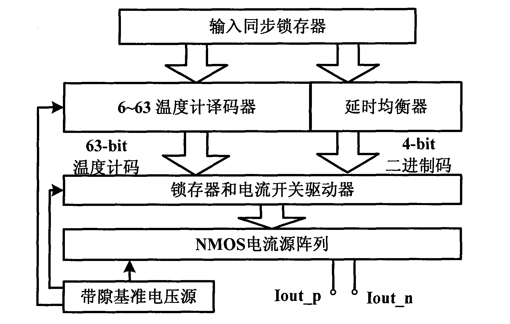
[0029] One. Design principle of the present invention

[0030] The MOS current mode logic used in the present invention has smaller power consumption delay product, adjustable output swing, and can maintain higher speed under low power supply voltage operation.

[0031] The output swing of an MCML circuit can be expressed as:

[0032] ΔV=I×R P (1)

[0033] Among them, I is the bias current value flowing through the branch, and R P is the resistance value of the adjustable resistor. It can be known from formula (1) that the output swing is adjusted by adjusting the current value or the resistance value. In order to ensure the normal operation of the circuit, the resistance value R P Make adjustments so that the current value I does not change.

[0034] In order to obtain a smaller ΔV, MOS current mode logic circuits often use MOS tubes operating in the deep linear region as loads to obtain smaller resistors with adjustable resistance. The channel resi...


PUM


Abstract

The invention discloses a CMOS digital to analog converter, mainly aiming to solve the problems of large switch noise, poor circuit precision and low speed of the traditional CMOS digital to analog converter under the condition of low power consumption. The CMOS digital to analog converter is composed of an input synchronization latch, a thermometer decoder, a delay equalizer, a latch, a current switch driver, an NMOS current source array and a band-gap reference voltage source, wherein the thermometer decoder adopts a parallel thermometer decoder structure and consists of an AND gate / NAND gate logical unit and an OR gate / NOR gate logical unit of an MOS current mode logical structure; the delay equalizer comprises a reverse directional device of the MOS current mode logic structure; both the latch and the current switch driver adopt the MOS current mode logic structure; and the input end of the NMOS current source array is connected with the complementary output ends of the latch and the current switch driver so as to generate complementary output current. The CMOS digital to analog converter in the invention has the advantages of small output pendulum deflection and switch noise, high circuit precision and rapid working speed, and can be applicable to communication, signal processing and video processing systems.

Description

technical field [0001] The invention belongs to the field of microelectronics, in particular to a CMOS digital-to-analog converter used in communication, signal processing and video processing systems. Background technique [0002] The continuous development of modern communication systems, information processing systems and video processing systems has prompted digital-analog hybrid circuit designers to devote themselves to the research of high-speed data converter IP cores. Among them, the embedded application of digital-to-analog converters in HDTV, mobile communication and other fields makes the design of high-speed and low-power consumption an important direction for the development of modern digital-to-analog converters. [0003] A traditional CMOS digital-to-analog converter consists of an input synchronous latch, a thermometer decoder and a delay equalizer, a latch and current switch driver, an array of NMOS current sources, and a bandgap reference voltage source. Th...

Claims


Application Information

Patent Timeline
Patent Type & Authority Applications(China)
IPC IPC(8): H03M1/66
Inventor 朱樟明杨银堂程武刘帘曦
Owner XIDIAN UNIV
Why Eureka
Try Eureka