Non-aperture tip enhanced Raman scattering probe and manufacturing method thereof

A tip-enhanced Raman and Raman scattering technology, applied in Raman scattering, material excitation analysis, etc., can solve the problems of rough surface of the tip, large radius of curvature of the tip of the tip, and difficulty in making TERS probes, etc., to increase image quality Effects of resolution, increased electromagnetic field strength, and high image spatial resolution

Active Publication Date: 2010-12-22
SHANGHAI INST OF CERAMIC CHEM & TECH CHINESE ACAD OF SCI
View PDF0 Cites 32 Cited by
  • Summary
  • Abstract
  • Description
  • Claims
  • Application Information

AI Technical Summary

Problems solved by technology

However, the tip surface of several Au and Ag widely used today is relatively rough, and the radius of curvature of the tip tip is relatively large. It is difficult to make a TERS probe with a tip diameter of less than 40 nanometers by conventional methods.

Method used


Image

  • Non-aperture tip enhanced Raman scattering probe and manufacturing method thereof
  • Non-aperture tip enhanced Raman scattering probe and manufacturing method thereof
  • Non-aperture tip enhanced Raman scattering probe and manufacturing method thereof

Examples


Embodiment 1

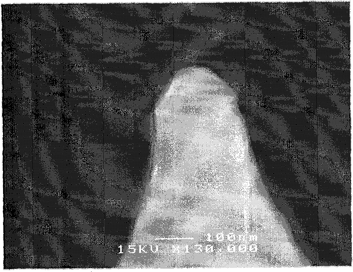
[0043] Magnetron sputtering (ULVAC, MPS-2000-HC3) was used to coat a silver film on the AFM silicon probe of Seiko Company in Japan, and a 99.99% high-purity silver target was sputtered in a high-purity (99.995%) argon gas. Before sputtering, the probe was ultrasonically cleaned in ethanol for 15 min with a working vacuum of 2 × 10 -6 Pa, sputtering time 100s, silver film thickness 100nm.

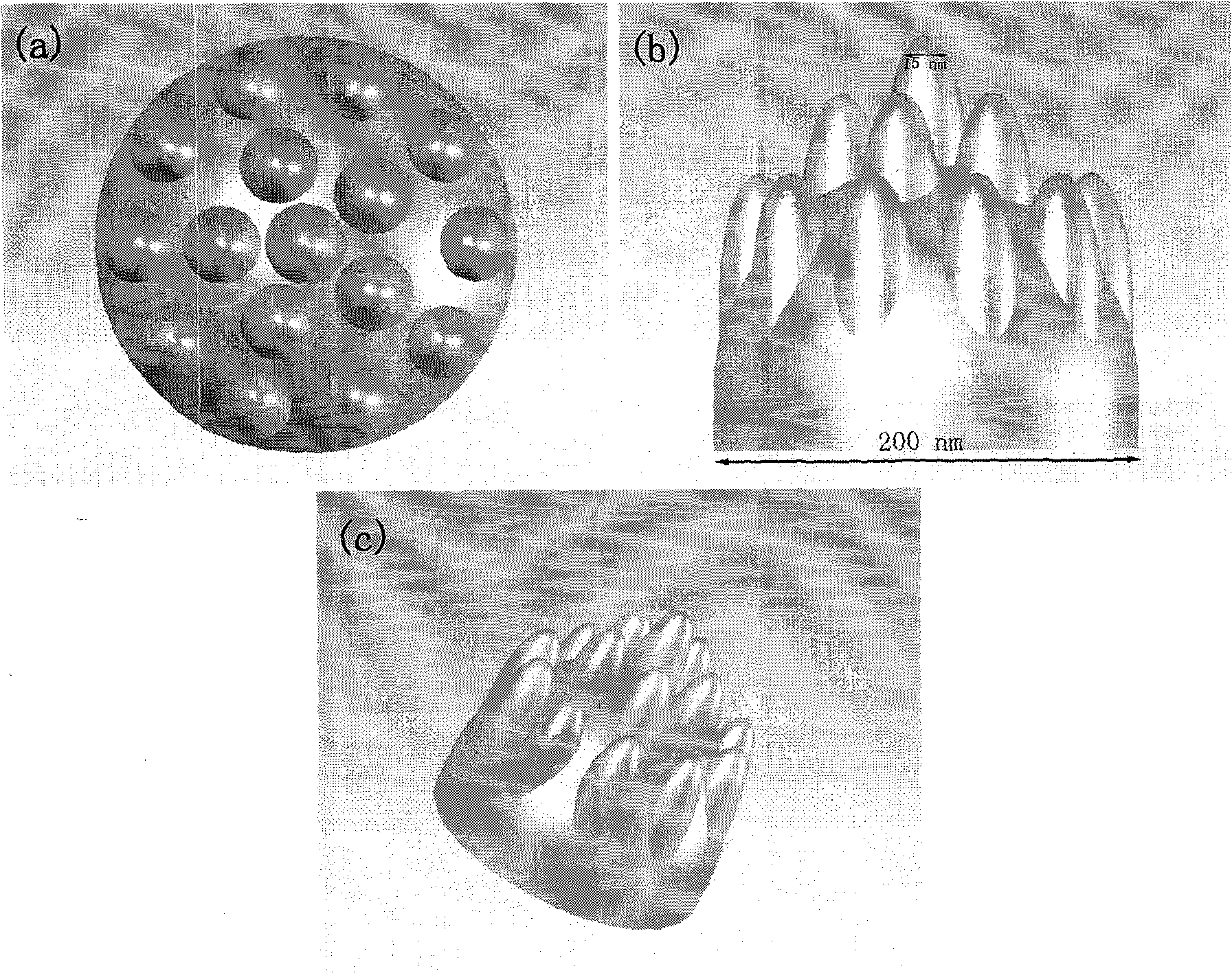
[0044] A carbon film layer is evaporated on the silver film layer as an "induction template" to induce the formation of pyramidal nanostructures, and the thickness is controlled at about 100nm.

[0045]The above-mentioned probe coated with silver film and carbon film was put into an ion beam system equipped with an ultra-high vacuum and a Kaufman-type ion gun. Among them, the 600eV argon ion beam is focused into a microbeam with a diameter of 380um, and its average ion current density is 220uA / cm 2 . The angle between the ion beam and the needle axis can be adjusted to 45 degrees by chan...

Embodiment 2

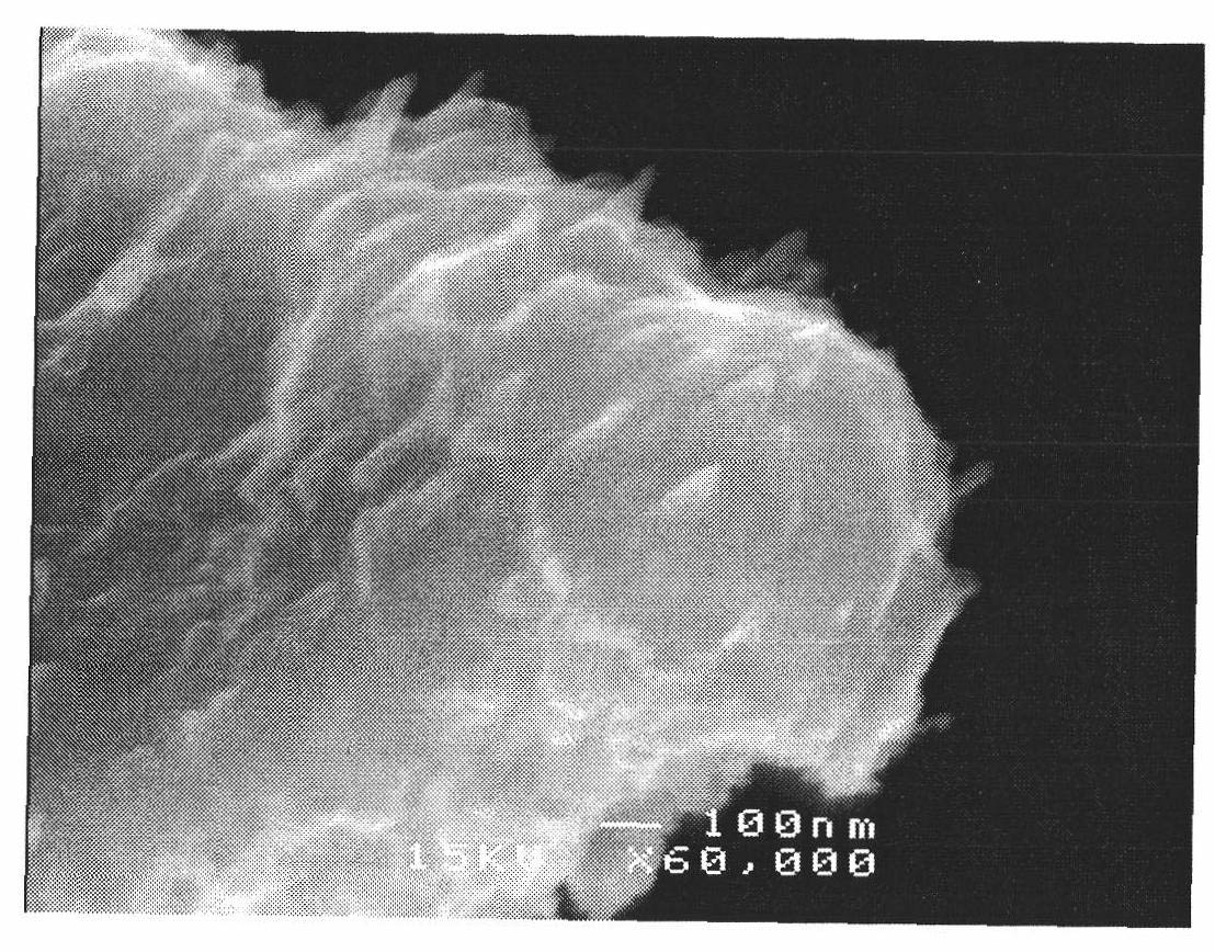
[0048] Magnetron sputtering (ULVAC, MPS-2000-HC3) was used to plate silver film on the AFM silicon probe of Japan Seiko Company, and the 99.99% high-purity silver target was sputtered in high-purity (99.995%) argon gas. Before sputtering, the probe was ultrasonically cleaned in ethanol for 15 minutes, and the working vacuum was 2×10 -6 Pa, the sputtering time is 200s, and the silver film thickness is 200nm.

[0049] A carbon film layer is deposited on the silver film layer as an "inducing template" to induce the formation of pyramidal nanostructures, and its thickness is controlled at about 100nm.

[0050] The above-mentioned probe coated with silver film and carbon film was put into an ion beam system equipped with an ultra-high vacuum and a Kaufman-type ion gun. Among them, the 600eV argon ion beam is focused into a microbeam with a diameter of 380um, and its average ion current density is 220uA / cm 2 . The angle between the ion beam and the sample surface can be adjusted ...


PUM

PropertyMeasurementUnit
diameteraaaaaaaaaa
diameteraaaaaaaaaa
thicknessaaaaaaaaaa

Abstract

The invention relates to a non-aperture tip enhanced Raman scattering probe and a manufacturing method thereof, belonging to the field of near-field Raman spectroscopy detection technology. The non-aperture tip enhanced Raman scattering probe is characterized in that the surface of the traditional Raman scattering probe is provided with 3-20 tiny tips, the diameter of the tiny tips is 5-25 nm, and the curvature radius of the tiny tips is 2-15 nm. In the invention, a scanning probe microscopy / atomic force microscopy (SPM / AFM) probe with a noble metal film layer is selected, a carbon layer is deposited on the noble metal film layer, and excess carbon layers are removed by washing after the impact of an argon ion beam. The manufactured non-aperture tip enhanced Raman scattering probe has great application potential in the fields of trace analysis, qualitative detection even single-molecule detection and the like.

Description

technical field [0001] The invention relates to a non-aperture needle tip enhanced Raman scattering probe and a preparation method thereof, belonging to the technical field of near-field Raman spectrum detection. Background technique [0002] Since 2000, scientists from Germany and Japan have introduced near-field optical microscopes into Raman spectroscopy technology, which has been developed into Tip-Enhanced Raman Spectroscopy (TERS), which can realize the measurement of material morphology and nanometer scale. The observation of near-field Raman signals makes near-field Raman spectroscopy one of the most advantageous tools for characterizing nanostructures, single molecules, and living organisms. Using TERS not only obtains high spatial resolution, but also obtains high detection sensitivity that is difficult to obtain with scanning near-field microscopy. [0003] The basic principle of TERS is to attach a very sharp Ag or Au tip with a radius of curvature of several te...

Claims


Application Information

Patent Timeline
Patent Type & Authority Applications(China)
IPC IPC(8): G01N21/65
Inventor 杨勇黄政仁野比上行钟村荣
Owner SHANGHAI INST OF CERAMIC CHEM & TECH CHINESE ACAD OF SCI
Why Eureka
Try Eureka