Method for preparing nitrogen-yttrium-zirconium hard coating with nano structure on surface of hard alloy substrate
A cemented carbide substrate and nanostructure technology, which is applied in the direction of metal material coating process, coating, ion implantation plating, etc., can solve the problems that are difficult to meet the needs of modern industry
- Summary
- Abstract
- Description
- Claims
- Application Information
AI Technical Summary
Problems solved by technology
Method used
Image
Examples
Embodiment 1
[0020] 1. Substrate pretreatment:
[0021] (1) Grinding and polishing: Carry out sufficient rough grinding and fine grinding of the cemented carbide substrate on 600 mesh and 1200 mesh diamond grinding wheel discs respectively. The sample must be fully ultrasonically cleaned (ultrasonic cleaning time is 2min) and dried in an oven to remove wear debris and oil stains; after the sample is ground, it is polished with W2.5 diamond polishing powder. The polishing time is 10min.
[0022] (2) Ultrasonic cleaning: Clean the polished substrate in the following order, ultrasonic cleaning with acetone for 5 minutes → ultrasonic cleaning with absolute ethanol for 5 minutes → drying for later use.
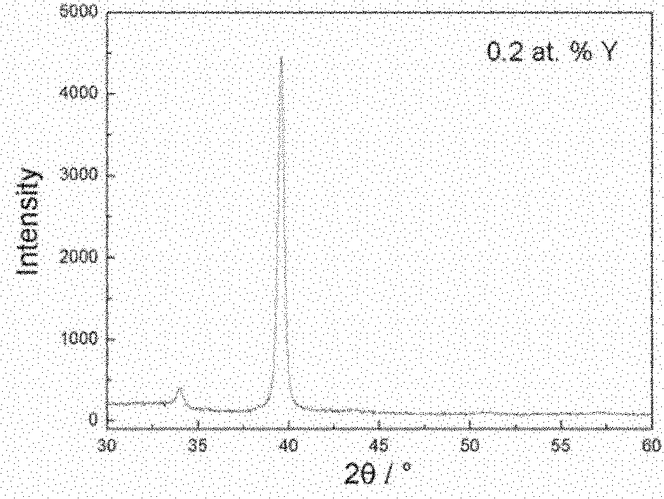
[0023] (3) Ion source cleaning: Before sputtering deposition, the Hall ion source is used to clean the substrate, and the pressure of ion cleaning is 2×10 -2 Pa, substrate temperature 300°C, argon flux 10sccm, bias voltage negative 100V, cathode current voltage 29.5A, 19V, anode current volta...
Embodiment 2
[0030] 1. Substrate pretreatment: same as embodiment 1.
[0031] 2. Pre-sputtering: same as embodiment 1.
[0032] 3. Sputtering deposition: After the pre-sputtering, argon and nitrogen are introduced, the total flux is 60sccm, of which the nitrogen flow rate is 20%, the working pressure of the deposition is 0.3Pa, the DC power supply of the Zr target is 250W, Y The RF power of the target is 100W, the sputtering time is 90min, and the substrate temperature is 300°C. After the deposition is complete, the sample is taken out and stored in a desiccator, pending characterization and analysis. After the deposition is complete, the sample is taken out and stored in a desiccator, pending characterization and analysis.
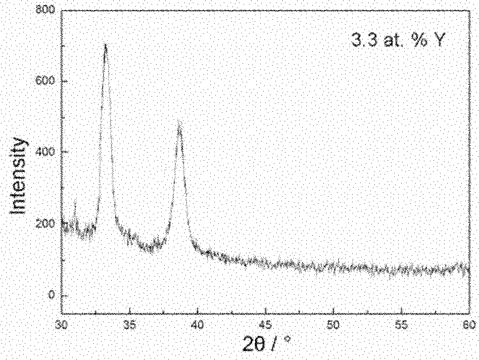
[0033] image 3 It is the XRD spectrum of the coating, which shows that the prepared coating has a face-centered cubic structure. The coating grain size test method is the same as in Example 1, and the coating grain size is calculated to be 17nm.
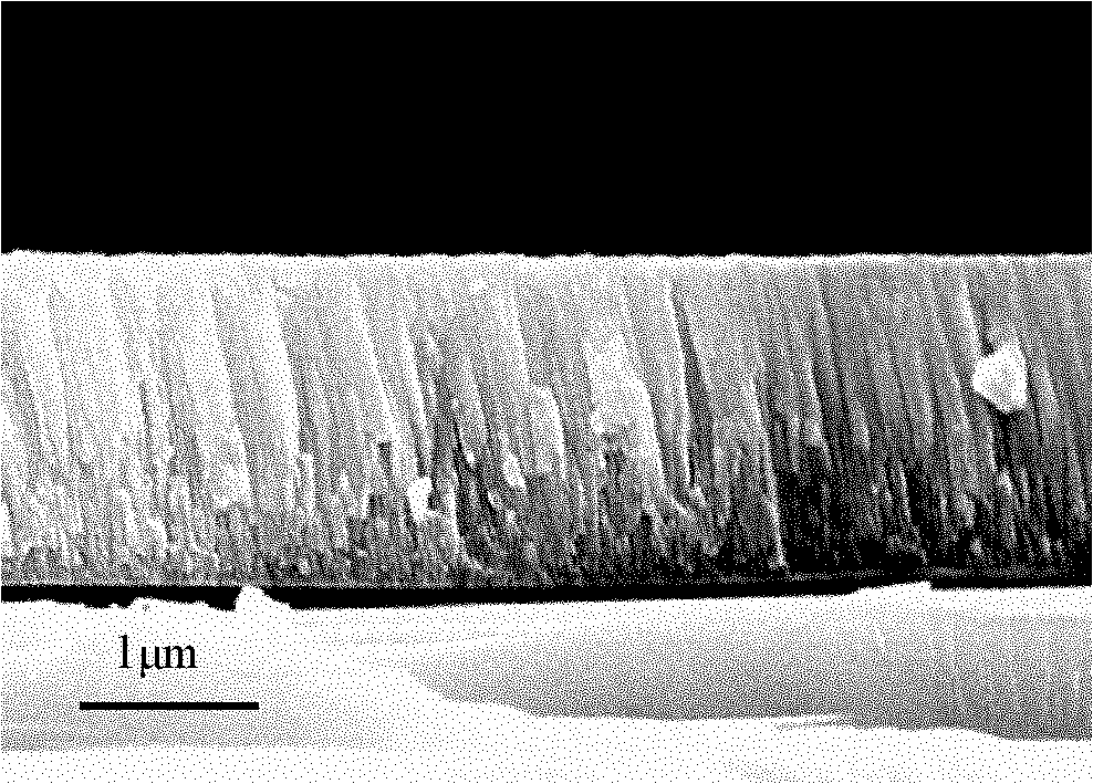
[0034] 4. The ...
Embodiment 3
[0037] 1. Substrate pretreatment: (1) Grinding and polishing: Same as Example 1. (2) ultrasonic cleaning: with embodiment 1. (3) Ion source cleaning: Same as in Example 1.
[0038] 2. Pre-sputtering: same as embodiment 1.
[0039] 3. Sputtering deposition: After the pre-sputtering, argon and nitrogen are introduced, the total flux is 60sccm, of which the nitrogen flow rate is 15%, the working pressure of the deposition is 0.4Pa, the DC power of the Zr target is 250W, Y The RF power of the target is 150W, the sputtering time is 90min, and the substrate temperature is 300°C. After the deposition is complete, the sample is taken out and stored in a desiccator, pending characterization and analysis. After the deposition is complete, the sample is taken out and stored in a desiccator, pending characterization and analysis.
[0040] Figure 4 It is the XRD spectrum of the coating, indicating that the prepared coating is a coating with a face-centered cubic structure. The coati...
PUM
| Property | Measurement | Unit |
|---|---|---|
| particle size | aaaaa | aaaaa |
| hardness | aaaaa | aaaaa |
| particle size | aaaaa | aaaaa |
Abstract
Description
Claims
Application Information


