
Anti-fatigue phase change storage unit with low power consumption and preparation method thereof

A phase-change storage and anti-fatigue technology, applied in electrical components, circuits, semiconductor devices, etc., can solve problems affecting voltage/current matching, operating voltage/current increase, device reliability threats, etc., to reduce power consumption, reduce Small stress changes, the effect of improving device stability

Active Publication Date: 2010-12-29
SHANGHAI INST OF MICROSYSTEM & INFORMATION TECH CHINESE ACAD OF SCI
View PDF2 Cites 10 Cited by
  • Summary
  • Abstract
  • Description
  • Claims
  • Application Information

AI Technical Summary

Problems solved by technology

The loss of too much heat through the bottom electrode will inevitably lead to an increase in the operating voltage / current during the phase transition process, and the energy consumption will increase accordingly, which will affect the voltage / current matching with the CMOS, and the excessive heat that spreads to the bottom of the device will affect the bottom of the device. The stability of CMOS operation is a potential detriment
In addition, in the phase change material containing Sb and Te elements, in the process of phase change operation, long-term repeated high-temperature writing and erasing operations will cause the composition segregation inside the material itself, and Sb or Te will segregate to the interface and interact with the active The phenomenon of electrode material reaction has also been proven to be a great threat to device reliability

Method used


Image

  • Anti-fatigue phase change storage unit with low power consumption and preparation method thereof
  • Anti-fatigue phase change storage unit with low power consumption and preparation method thereof
  • Anti-fatigue phase change storage unit with low power consumption and preparation method thereof

Examples


Embodiment Construction

[0029] The invention is described more fully below with reference to the drawings, which provide preferred embodiments, but should not be considered limited to the embodiments set forth herein. In the figure, the thicknesses of layers and regions are appropriately enlarged for a clearer reaction structure, but as a schematic diagram, it should not be considered to strictly reflect the proportional relationship of geometric dimensions. The referenced figures are schematic views of the present invention, and the representations in the figures are only schematic in nature and should not be considered as limiting the scope of the present invention.

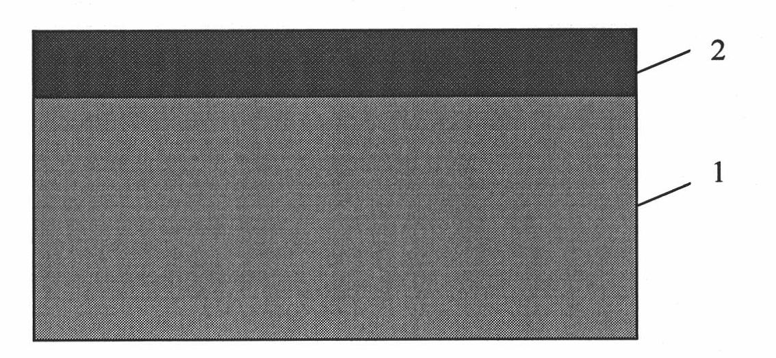
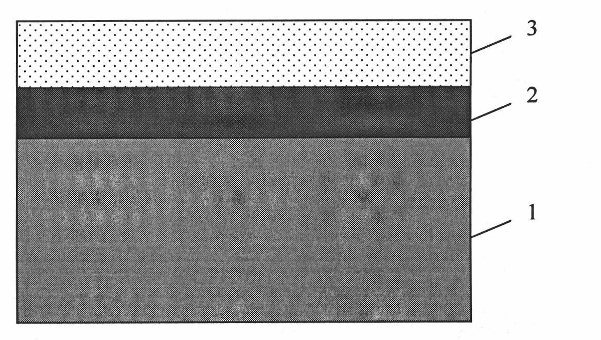
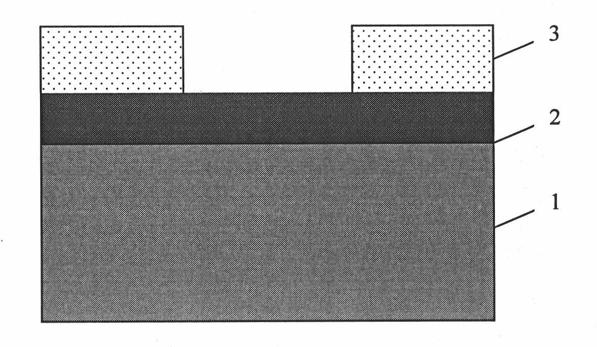
[0030] The low power consumption anti-fatigue phase change memory unit of the present invention comprises in turn: a semiconductor substrate, a lower electrode layer located on the semiconductor substrate, a dielectric material transition layer located on the lower electrode, a dielectric material transition layer located on the A com...


PUM

PropertyMeasurementUnit
thicknessaaaaaaaaaa
thicknessaaaaaaaaaa

Abstract

The invention discloses an anti-fatigue phase change storage unit with low power consumption, comprising a lower electrode, a dielectric material transition layer located above the lower electrode, a composite phase change material layer located above the dielectric material transition layer and an upper electrode located above the composite phase change material layer. The dielectric material transition layer adopts a first dielectric material which is one or more of Ta2O5, TiO2 and CeO2; and the composite phase change material layer adopts a composite material consisting of a phase change material and a second dielectric material which is one or more of SiO2, HfO2, Ta2O5, TiO2 and CeO2. The invention also provides a method for preparing the anti-fatigue phase change storage unit with low power consumption; the phase change storage unit can reduce the heat loss, prevent the phase change material volatilization, improve the heat stability, optimize the interface and decrease the stress change before and after the phase change; therefore, the phase change storage unit is beneficial for the stability of the device performance, on one hand, the power consumption of the device is reduced, on the other hand, the anti-fatigue characteristic of the device is improved.

Description

technical field [0001] The invention relates to a phase-change storage unit and a preparation method thereof, in particular to a low-power-consumption and anti-fatigue phase-change storage unit and a preparation method thereof, belonging to the field of microelectronics nanometer materials and device preparation. Background technique [0002] Phase Change Memory (Phase Change Memory, PCM) is a new type of semiconductor memory, which uses chalcogenide compounds as storage media, and uses electric energy (heat) to make materials change between crystalline (low resistance) and amorphous (high resistance) The mutual conversion between them realizes the writing and erasing of information, and the reading of information is realized by measuring the change of resistance. Compared with a variety of semiconductor storage technologies currently available, including conventional volatile technologies, such as static random access memory (SRAM), dynamic random access memory (DRAM), etc....

Claims


Application Information

Patent Timeline
Patent Type & Authority Applications(China)
IPC IPC(8): H01L45/00H01L27/24
Inventor 宋三年宋志棠吕业刚
Owner SHANGHAI INST OF MICROSYSTEM & INFORMATION TECH CHINESE ACAD OF SCI
Learn More