Three-dimensional microheater with arc groove heating membrane area and manufacturing method thereof
An arc-shaped groove and heating film area technology, applied in the direction of heating element materials, microstructure technology, microstructure devices, etc., to achieve the effects of increasing reliability, easy arraying and mass production, and heat concentration
- Summary
- Abstract
- Description
- Claims
- Application Information
AI Technical Summary
Problems solved by technology
Method used
Image

Examples
Embodiment 1
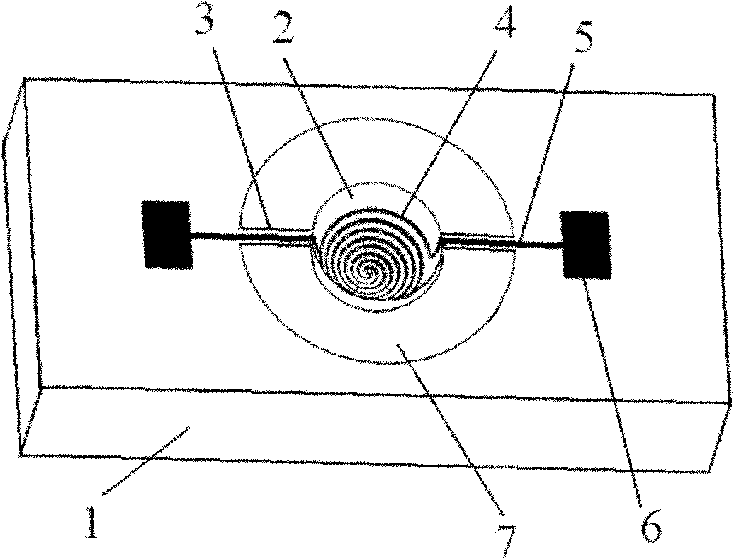
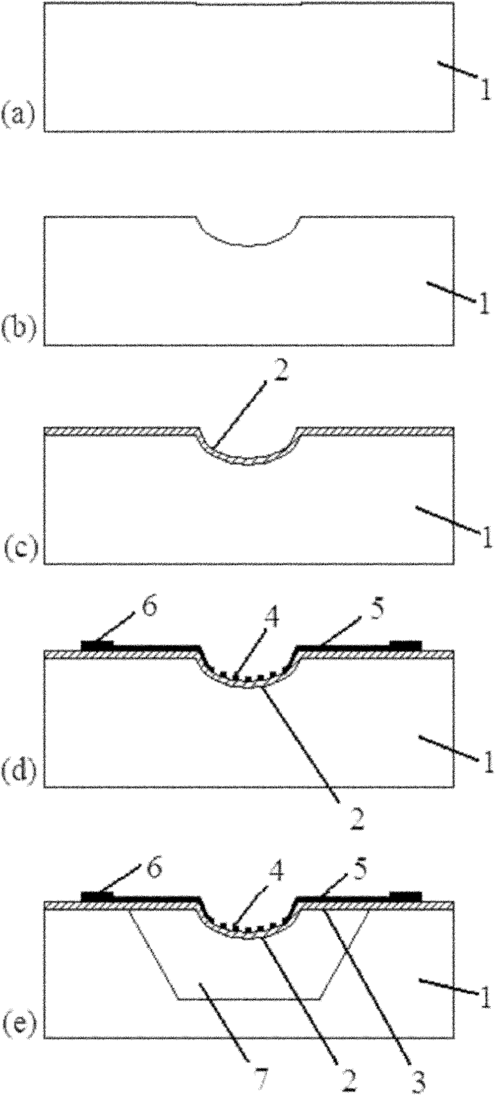
[0036] The structure diagram of this embodiment can be found in figure 1 As shown, the specific production method is as follows:
[0037] 1. Selection of silicon substrate: choose a 4-inch silicon wafer with an N-type (110) surface as the substrate, with a resistivity of 1-10Ω·cm, and a silicon wafer thickness of 450±10 microns.
[0038] 2. Making the front etching window for forming the groove structure: a silicon oxide film with a thickness of 2.0 microns is formed on the surface of the silicon wafer by thermal oxidation. Then perform photolithography to make a window pattern, and use reactive ion etching (RIE) to completely etch the exposed silicon oxide under the protection of the photoresist to form a front etching window.
[0039] 3. Make a groove with a circular arc-shaped cross-section: under the protection of silicon oxide, use the method of silicon isotropic dry etching to etch a circular arc-shaped groove on the silicon wafer through the etching window formed in s...
Embodiment 2
[0046] The structure diagram of this embodiment can be found in image 3 As shown, the specific production method is as follows:
[0047] 1. Selection of silicon substrate: choose a 4-inch silicon wafer with an N-type (100) plane as the substrate, with a resistivity of 3-8Ω·cm, and a silicon wafer thickness of 350±10 microns.
[0048] 2. Making the front etching window for forming the groove structure: a silicon oxide film with a thickness of 2.0 microns is formed on the surface of the silicon wafer by means of low-pressure chemical vapor deposition (LPCVD). Then perform photolithography to make a window pattern, and use ion beam etching (Ion-beam) to completely etch the exposed silicon oxide under the protection of the photoresist to form a front etching window.
[0049] 3. Make a groove with a circular arc-shaped cross-section: under the protection of silicon oxide, use the method of silicon isotropic dry etching to etch a circular arc-shaped groove on the silicon wafer thr...
Embodiment 3
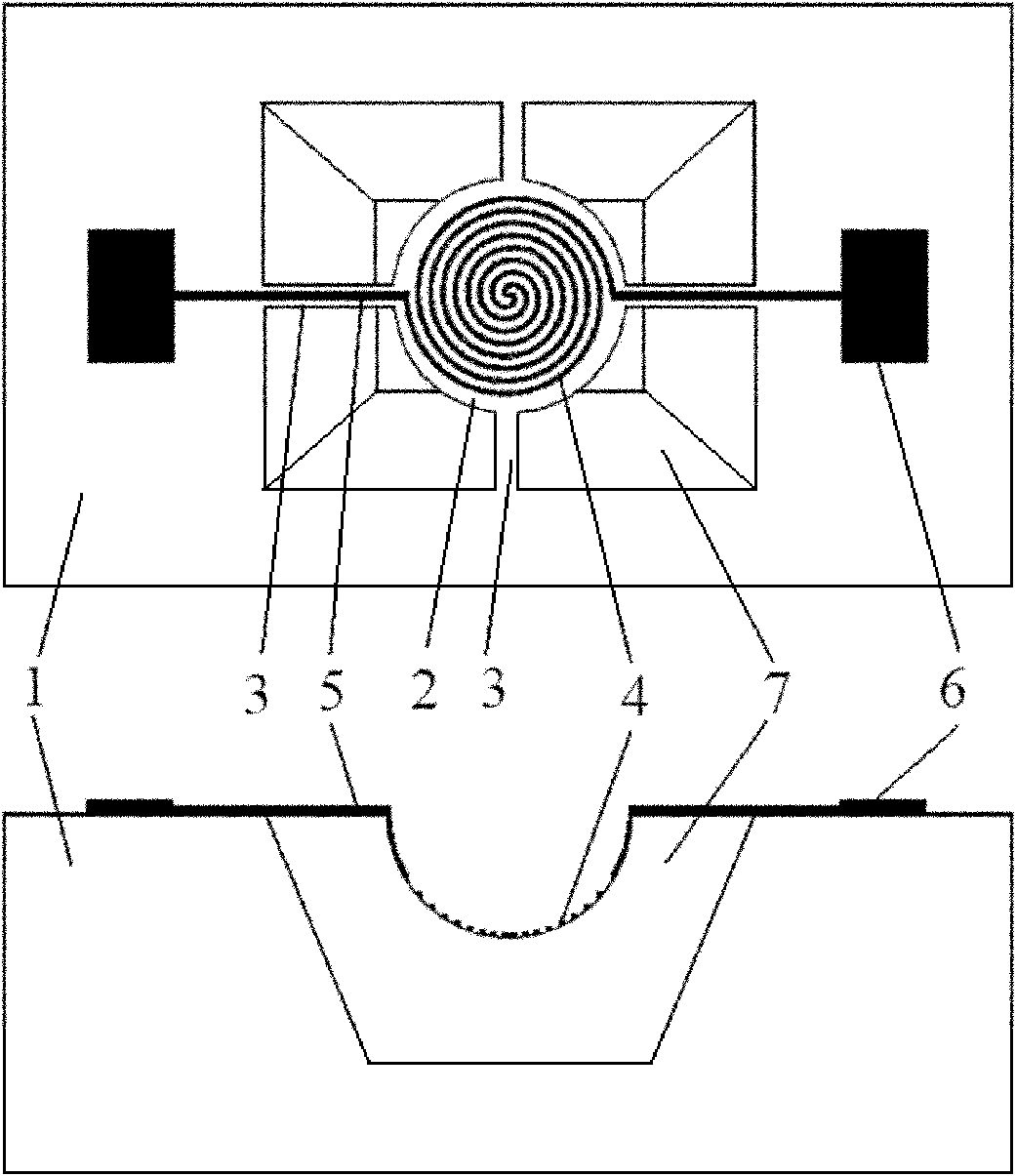
[0056] The structure diagram of this embodiment can be found in Figure 4 As shown, the specific production method is as follows:
[0057] 1. Selection of silicon substrate: select a 4-inch silicon wafer with a P-type (111) plane as the substrate, with a resistivity of 1-10Ω·cm, and a silicon wafer thickness of 450±10 microns.
[0058] 2. Making the front etching window for forming the groove structure: a silicon oxide film with a thickness of 1.0 micron is formed on the surface of the silicon wafer by thermal oxidation. Then perform photolithography to make a window pattern, and use ion beam etching (Ion-beam) to completely etch the exposed silicon oxide under the protection of the photoresist to form a front etching window.
[0059] 3. Make a groove with a circular arc-shaped cross-section: under the protection of silicon oxide, use the method of silicon isotropic dry etching to etch a circular arc-shaped groove on the silicon wafer through the etching window formed in step...
PUM
| Property | Measurement | Unit |
|---|---|---|
| Thickness | aaaaa | aaaaa |
| Depth | aaaaa | aaaaa |
| Thickness | aaaaa | aaaaa |
Abstract
Description
Claims
Application Information
 - R&D
- Intellectual Property
- Life Sciences
- Materials
- Tech Scout
- Unparalleled Data Quality
- Higher Quality Content
- 60% Fewer Hallucinations
Browse by: Latest US Patents, China's latest patents, Technical Efficacy Thesaurus, Application Domain, Technology Topic, Popular Technical Reports.
© 2025 PatSnap. All rights reserved.Legal|Privacy policy|Modern Slavery Act Transparency Statement|Sitemap|About US| Contact US: help@patsnap.com