

Method for preparing KTP rib optical waveguide by combining ion implantation with ion beam etching
A technology of ion beam etching and ion implantation, which is applied in the direction of light guides, optics, optical components, etc., and can solve the problem of making less ridge-shaped optical waveguides
- Summary
- Abstract
- Description
- Claims
- Application Information
AI Technical Summary
Problems solved by technology
Method used
Image

Examples
Embodiment 1
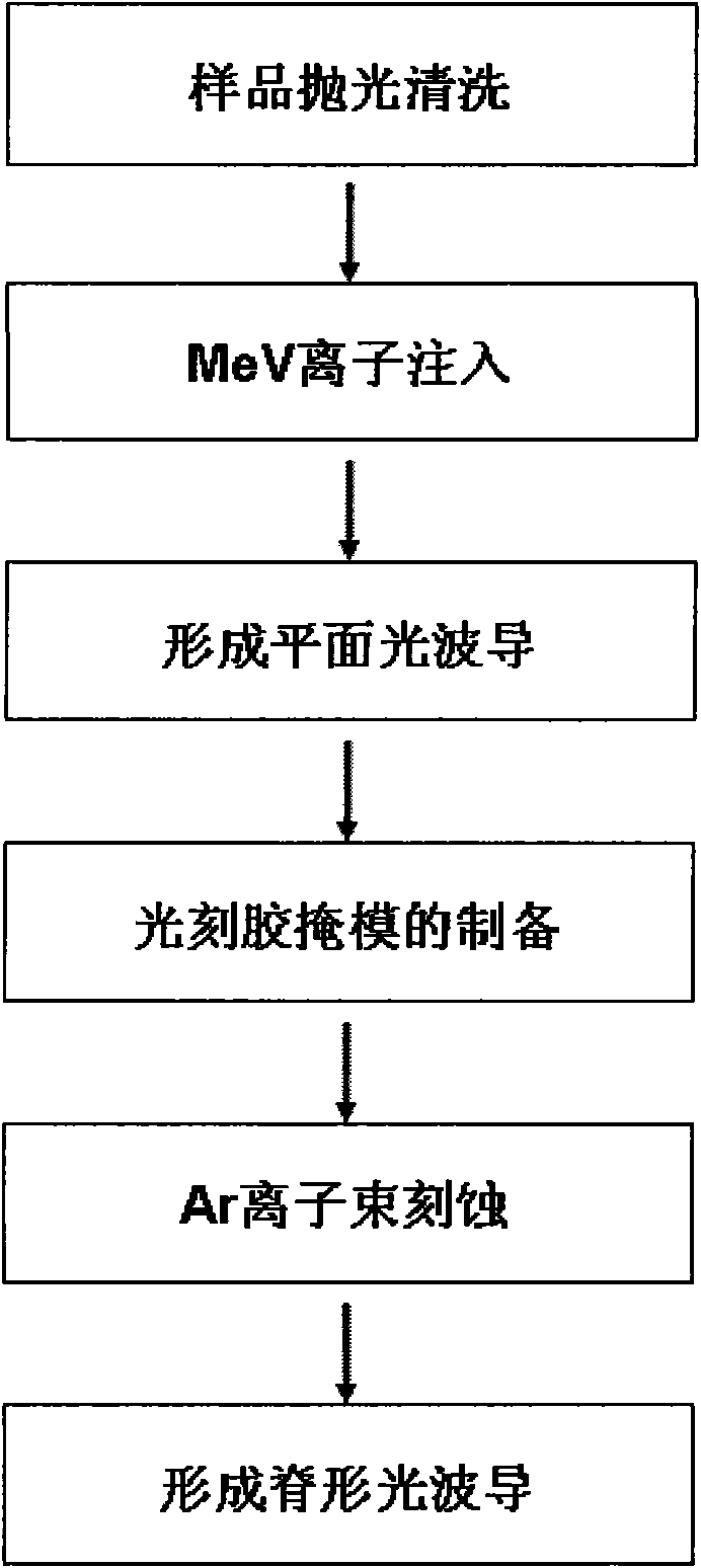
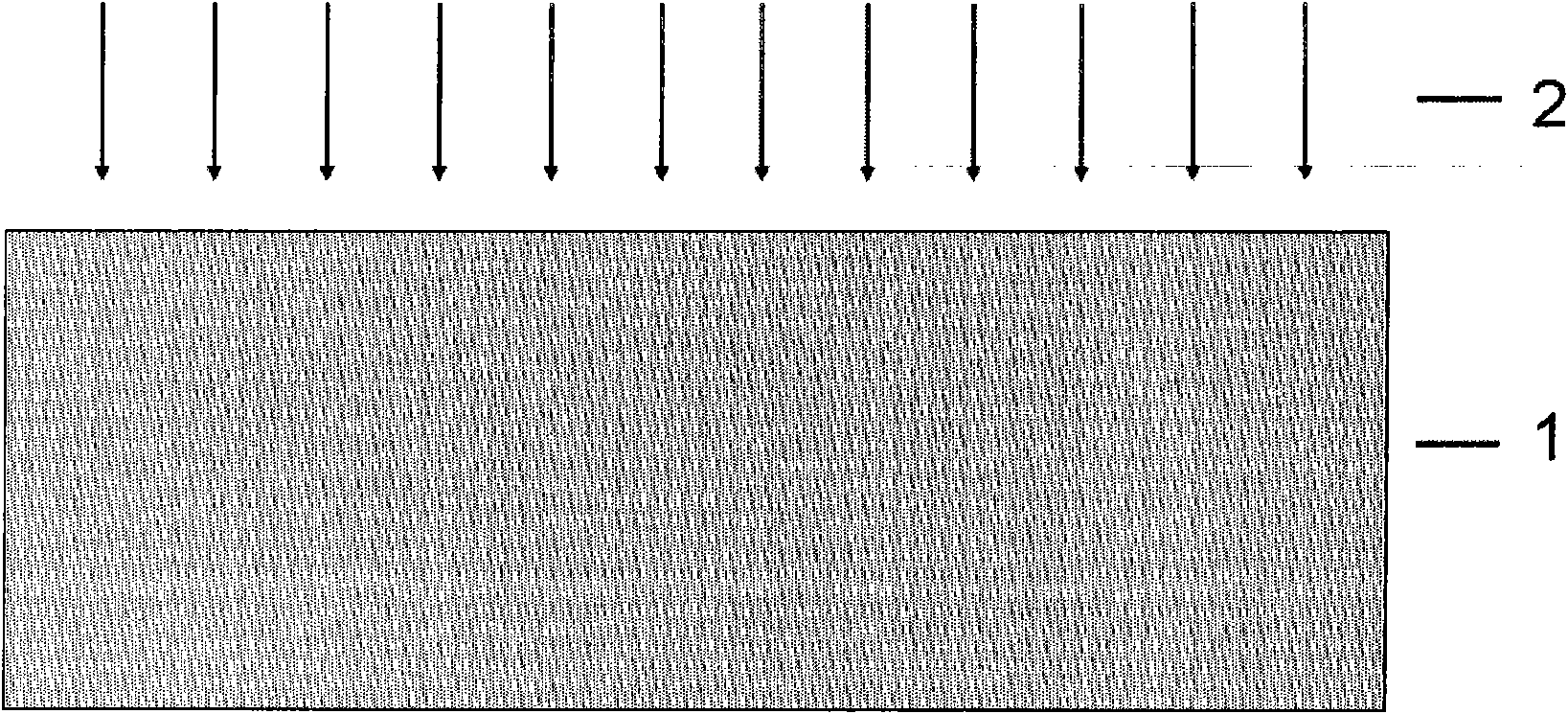
[0018] 1) Sample treatment: select the sample KTP crystal, Z-cut, the size is 10 mm × 8 mm, the thickness is 1.5 mm, the surface is optically polished; the sample is cleaned by acetone, deionized water and alcohol, and then prepared for ion implantation;
[0019] 2) Ion implantation: put the sample processed in step 1) in the accelerator target chamber, and vacuumize to 10 -4 Pascal level, ion implantation, the selected implantation conditions are: implanted ions: carbon ions, ion energy: 6.0MeV (megaelectron volts), implantation dose: 5×10 13 Ions / cm2, the ion beam current is 20 nanoamperes. The sample is implanted with ions to form a planar optical waveguide, and the planar optical waveguide is cleaned with acetone, deionized water and alcohol successively.
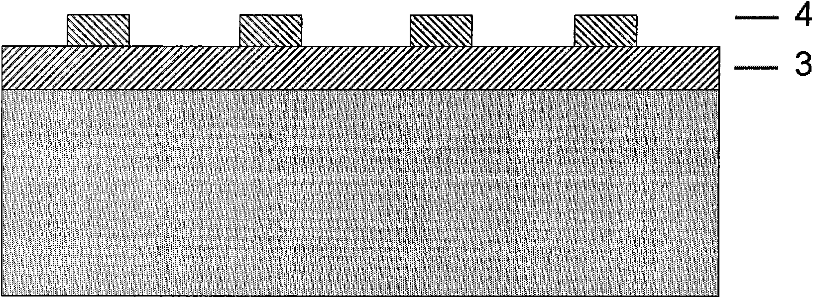
[0020] 3) Preparation of photoresist mask
[0021] Coating: Use a high-speed coating machine to coat photoresist on the cleaned KTP crystal planar optical waveguide at a speed of 5000 rpm and pre-bake at 120 degrees C...
Embodiment 2
[0027] 1) Sample treatment: select the sample KTP crystal, Z-cut, the size is 10 mm × 8 mm, the thickness is 1.5 mm, the surface is optically polished; the sample is cleaned by acetone, deionized water and alcohol, and then prepared for ion implantation;
[0028] 2) Ion implantation: put the sample treated in step 1) in the target chamber of the ion implanter, and vacuumize to 10 -4 Pascal level, perform ion implantation; select the implantation conditions as follows: implanted ions: helium ions, ion energy: 500keV, implantation dose: 1×10 15 Ions / cm2, the ion beam current is 100 nanoamperes. The sample is implanted with ions to form a planar optical waveguide, and the planar optical waveguide is cleaned with acetone, deionized water and alcohol successively.
[0029] 3. Photoresist Mask Preparation
[0030] Coating: Use a high-speed coating machine to coat photoresist on the cleaned KTP crystal planar optical waveguide at a speed of 5000 rpm and pre-bake at 120 degrees Cels...
PUM
 Abstract
Description
Claims
Application Information