
Method for removing light-emitting diode (LED) chip electrode

A LED chip and electrode technology, which is applied in circuits, electrical components, semiconductor devices, etc., can solve the problems of P-type GaN surface damage, high forward voltage of products, and material consumption. The method is simple, highly selective, and The effect of guaranteeing quality

Inactive Publication Date: 2011-01-12
XIANGNENG HUALEI OPTOELECTRONICS
View PDF5 Cites 27 Cited by
  • Summary
  • Abstract
  • Description
  • Claims
  • Application Information

AI Technical Summary

Problems solved by technology

There are two disadvantages in this method: one is that there are too many rework processes, time-consuming and material-consuming; the other is that the ITO conductive film in the chip and the P-type GaN have been annealed, and the GaN surface and ITO have been well integrated , if the original ITO layer is washed off by strong acid immersion during the electrode removal process, it is very likely that the P-type GaN surface at this time will be damaged, and it will not be well integrated with the second evaporated ITO film, eventually resulting in the product The forward voltage is high, especially for roughened epitaxial wafers.
But this method cannot remove the remaining Cr and Pt in the electrode, and its production practicability is not very good

Method used

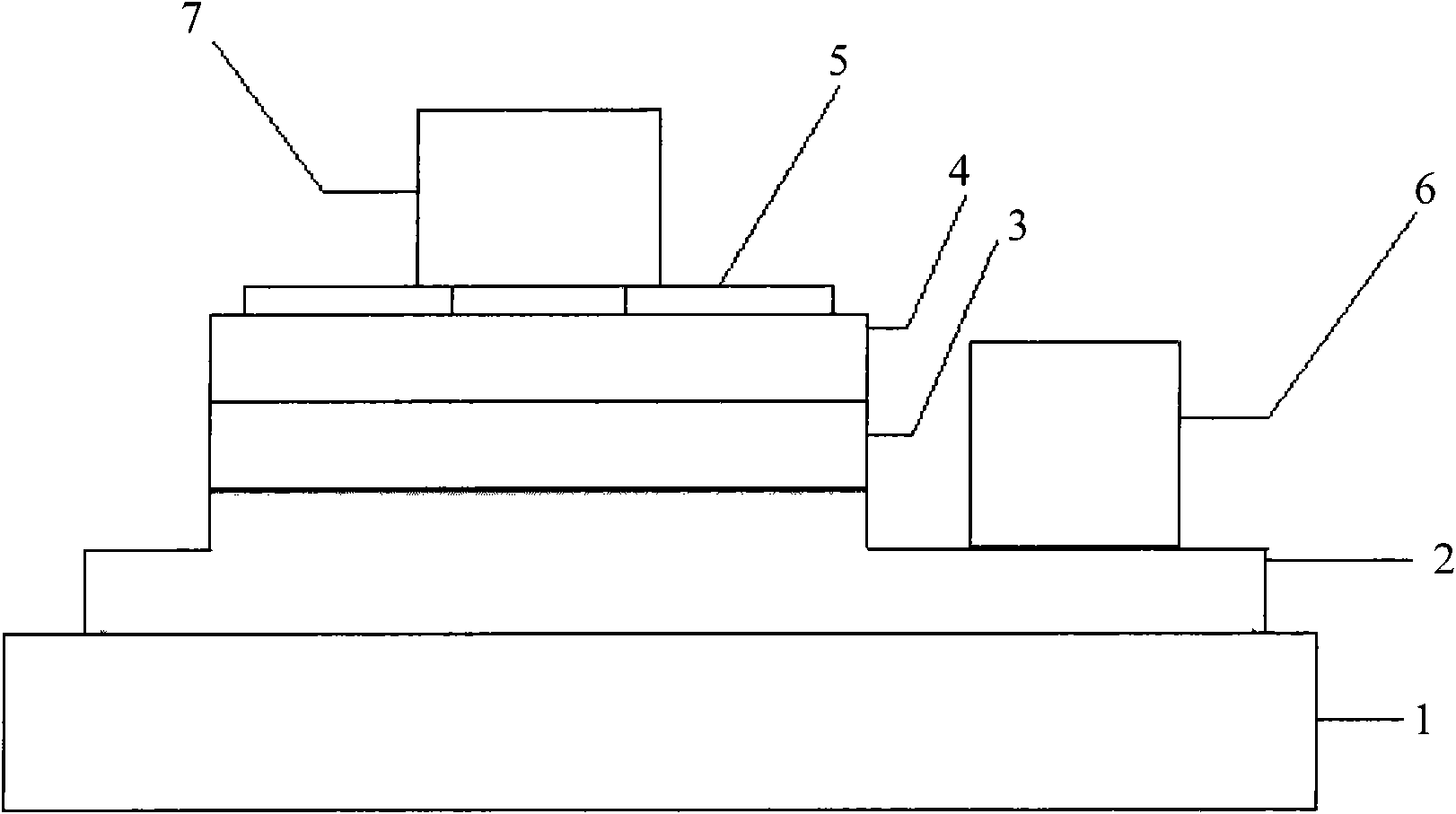
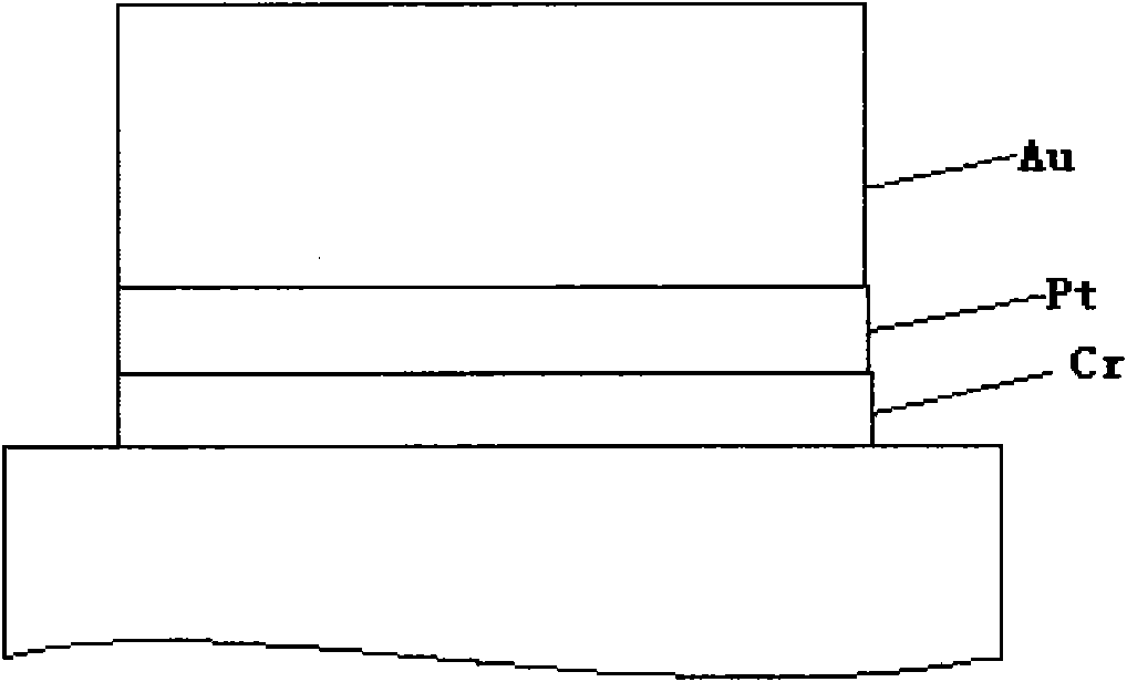
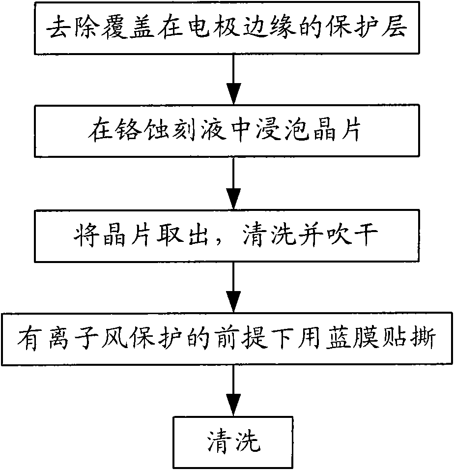

Image

  • Method for removing light-emitting diode (LED) chip electrode
  • Method for removing light-emitting diode (LED) chip electrode
  • Method for removing light-emitting diode (LED) chip electrode

Examples


Embodiment

[0038] According to the electrode removal method provided by the present invention, a rework process was carried out on 100 chips, and the forward voltage value of the chips was tested. During the rework process, the mass percent of the chromium etching solution used is 15%, and the pH is weakly acidic. Ultrasonic oscillation is performed while soaking the chip, and the blue film is used to peel off. After the above electrode removal process, PAD photolithography, electrode evaporation, and stripping are performed to complete the entire rework process. The test shows that the forward voltage values ​​​​of these 100 chips are within the normal range, and there is no deviation from the normal value.

[0039] As can be seen from the above steps, the LED chip electrode removal method provided by the present invention has the following advantages and positive effects:

[0040] 1. Save time and materials

[0041] The traditional removal method is: removal of electrodes and ITO→eva...


PUM


Abstract

The invention discloses a method for removing an LED chip electrode, which comprises the following steps of: removing a protective layer covered on the edge of the LED chip electrode; immersing the chip in chrome etching liquid after the protective layer is removed; taking the immersed chip out, washing and drying by air; and adhering a blue membrane or a white membrane on the surface of the air dried chip and then peeling the blue membrane or the white membrane off. The method provided by the invention has very high selectivity, exerts no influences on the other parts of the LED chip structure and retains the conventional indium tin oxide (ITO) layer.

Description

technical field [0001] The invention belongs to the field of LED chip manufacture, and in particular relates to a method for removing LED chip electrodes. Background technique [0002] Light-emitting diode (LED) is a semiconductor device that can convert electrical energy into light energy, and has been widely used in various fields such as urban beautification, indicator display, and indoor lighting. The LED generates photons by injecting current between the two electrodes, and electrons recombine with holes in the quantum well of the LED. [0003] There are roughly three types of substrate materials for LED chips, sapphire, silicon, and silicon carbide. The LED chip with sapphire as the substrate refers to GaN-based materials and the epitaxial layer of the device are mainly grown on the sapphire substrate. The LED chip uses ITO film with good conductivity and light transmission performance as the N-type GaN conductive layer, and the two electrodes are formed by sequentia...

Claims


Application Information

Patent Timeline
Patent Type & Authority Applications(China)
IPC IPC(8): H01L33/00
Inventor 谈健许亚兵林振贤何大庆
Owner XIANGNENG HUALEI OPTOELECTRONICS
Learn More