

Fractal graphene material with negative electron affinity as well as preparation method and application thereof
An affinity and graphene technology, applied in the field of fractal graphene materials, can solve the problems of poor emission uniformity and low efficiency, and achieve the effect of achieving density, overcoming low proportion, and improving low field emission capability.
- Summary
- Abstract
- Description
- Claims
- Application Information
AI Technical Summary
Problems solved by technology
Method used
Image

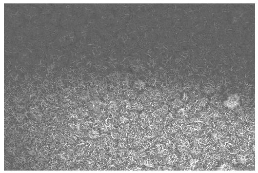
Examples
Embodiment 1
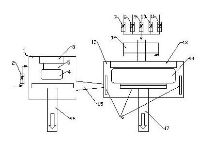
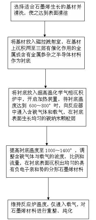
[0039] Such as figure 2 Shown, method of the present invention comprises the following steps:
[0040] 1) Select copper suitable for graphene growth as the substrate, and perform physical and chemical cleaning on the substrate to achieve the clean surface state required for deposition;
[0041] 2) Load the cleaned substrate into the magnetron sputtering reaction chamber 1, start the vacuum units 16 and 17, and wait until the vacuum degree reaches 8×10 -4 Pa, through the flow meter 2 into the inert gas, so that the vacuum rose to 1Pa and kept stable, start the electrode 3, the formation of plasma 4, through the plasma bombardment of the substrate 5, deposit three layers of nickel metal on the substrate as a lining end;
[0042] 3) After the deposition is completed, wait for the vacuum degree to return to 10 -3 Pa, the substrate deposited on the base material is sent into the ultra-high temperature chemical vapor deposition reaction chamber 18 by the transfer robot arm 15; t...
Embodiment 2
[0047] This embodiment includes the following steps:
[0048] 1) Select a semiconductor material (such as silicon) suitable for graphene growth as the substrate, and perform physical and chemical cleaning on the substrate to achieve the surface cleanliness required for deposition;
[0049] 2) Load the cleaned substrate into the magnetron sputtering reaction chamber 1, start the vacuum units 16 and 17, and wait until the vacuum degree reaches 8×10 -4 Pa, through the flow meter 2 into the inert gas, so that the vacuum rose to 1Pa and kept stable, start the electrode 3, the formation of plasma 4, through the plasma bombardment of the substrate 5, sequentially deposit cobalt-nickel metal on the substrate as a lining end;
[0050] 3) After the deposition is completed, wait for the vacuum degree to return to 10 -3 Pa, the substrate deposited on the base material is sent into the ultra-high temperature chemical vapor deposition reaction chamber 18 by the transfer robot arm 15; the ...
Embodiment 3
[0055] This embodiment includes the following steps:
[0056] 1) Select ceramics suitable for graphene growth as the substrate, and perform physical and chemical cleaning on the substrate to achieve the clean surface state required for deposition;
[0057] 2) Load the cleaned substrate into the magnetron sputtering reaction chamber 1, start the vacuum units 16 and 17, and wait until the vacuum degree reaches 8×10 -4 During Pa, feed inert gas through flow meter 2, make vacuum rise to 1Pa and keep stable, start electrode 3, form plasma 4, by plasma bombardment substrate 5, deposit cobalt-chromium-nickel metal successively on substrate as Substrate;
[0058] 3) After the deposition is completed, wait for the vacuum degree to return to 10 -3 Pa, the substrate deposited on the base material is sent into the ultra-high temperature chemical vapor deposition reaction chamber 18 by the transfer robot arm 15; the vacuum degree of the reaction chamber 18 reaches 5×10 -4 At Pa, start t...
PUM
 Abstract
Description
Claims
Application Information