Nitride semiconductor wafer, nitride semiconductor chip, method of manufacture thereof, and semiconductor device

A technology of nitride semiconductor and manufacturing method, applied in semiconductor/solid-state device manufacturing, semiconductor device, semiconductor laser, etc., can solve the problem of high luminous efficiency

Inactive Publication Date: 2011-03-30
SHARP KK
View PDF8 Cites 7 Cited by
  • Summary
  • Abstract
  • Description
  • Claims
  • Application Information

AI Technical Summary

Problems solved by technology

[0010] However, in the case of using the existing active layer structure described in Japanese Patent Application Laid-Open No. 2008-226865, it cannot be said that its luminous efficiency is sufficiently high, and there is still room for improving luminous efficiency.

Method used


Image

  • Nitride semiconductor wafer, nitride semiconductor chip, method of manufacture thereof, and semiconductor device
  • Nitride semiconductor wafer, nitride semiconductor chip, method of manufacture thereof, and semiconductor device
  • Nitride semiconductor wafer, nitride semiconductor chip, method of manufacture thereof, and semiconductor device

Examples


no. 1 approach

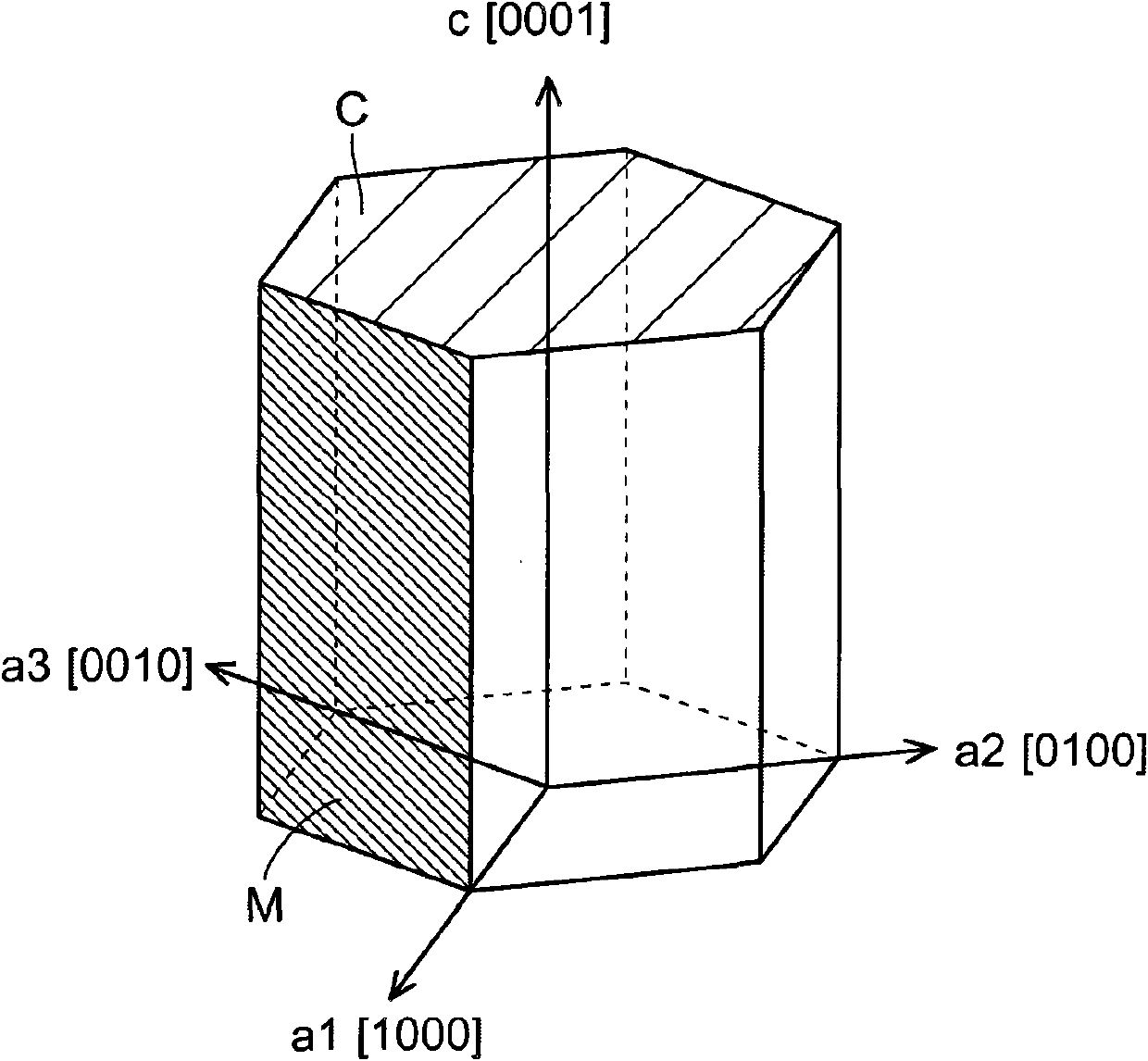
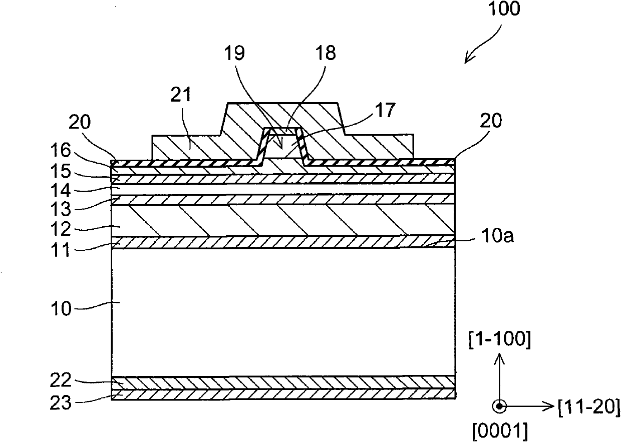
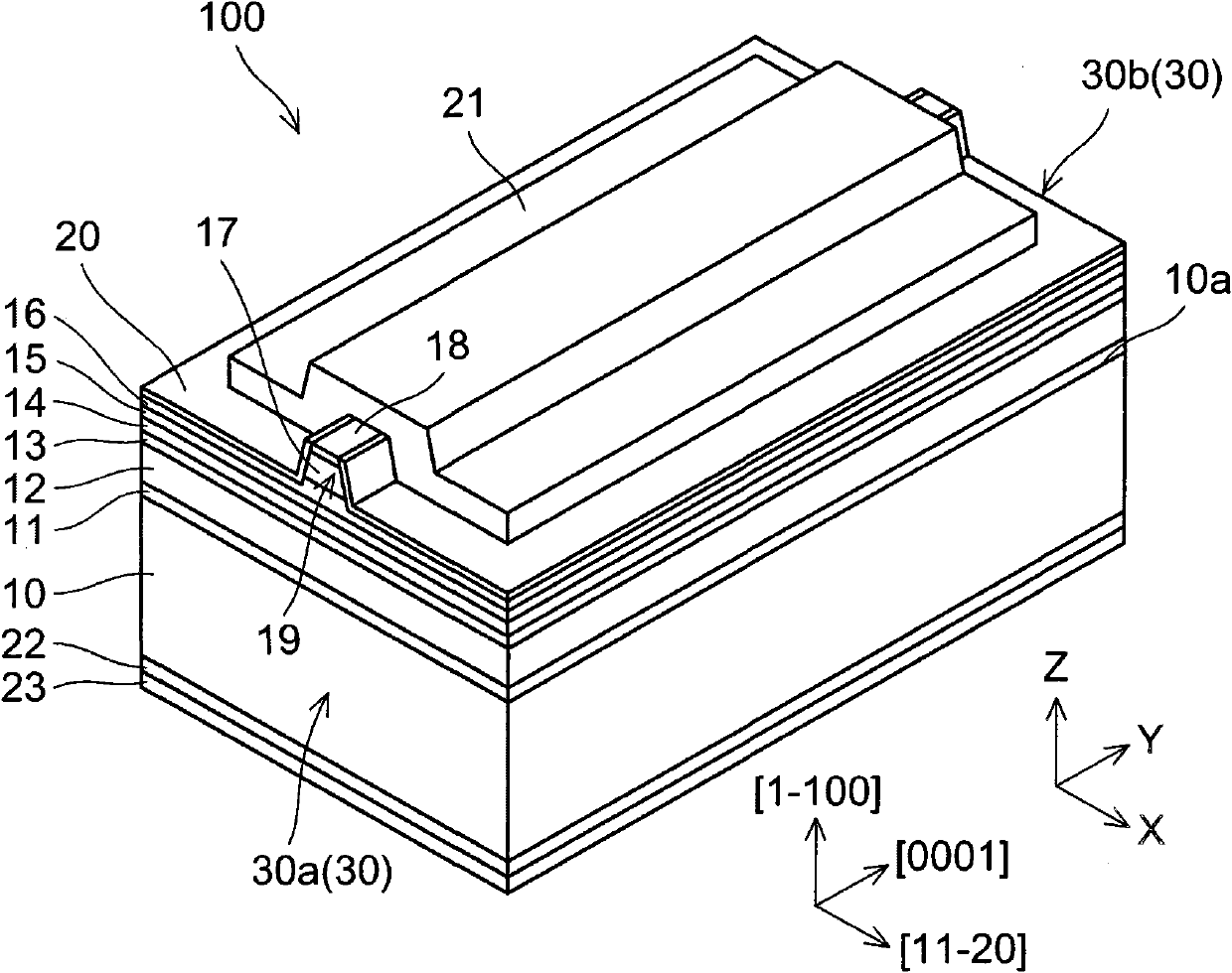
[0218] figure 1 It is a schematic diagram for explaining the crystal structure of a nitride semiconductor. figure 2 It is a cross-sectional view showing the structure of the nitride semiconductor laser device according to the first embodiment of the present invention. image 3 It is an overall perspective view of the nitride semiconductor laser device according to the first embodiment of the present invention. Figure 4 ~ Figure 6 It is a diagram for explaining the structure of the nitride semiconductor laser device according to the first embodiment of the present invention. First, refer to Figure 1 to Figure 6 The structure of the nitride semiconductor laser device 100 according to the first embodiment of the present invention will be described.

[0219] Such as figure 1 As shown, the nitride semiconductor constituting the nitride semiconductor laser device 100 of the first embodiment has a hexagonal crystal structure. In this crystal structure, the c-axis [0001] of th...

Embodiment 1

[0316] As the nitride semiconductor laser element of Example 1, a GaN substrate having an inclination angle of 1.7 degrees in the a-axis direction and +0.1 degrees in the c-axis direction with respect to the m-plane {1-100} was used, and the same as the above-mentioned first The nitride semiconductor laser device of the embodiment is the same as the nitride semiconductor laser device. The In composition ratio of the well layer was set to 0.25, and the Al composition ratio of the barrier layer was set to 2%. Other configurations of this first embodiment are the same as those of the above-mentioned first embodiment. In addition, a nitride semiconductor laser element produced in the same manner as the nitride semiconductor laser element of the first embodiment was used as a comparative example 1 using a GaN substrate (front m-plane substrate) having no off-angle. Other structures of the nitride semiconductor laser device of Comparative Example 1 are the same as those of Example ...

Embodiment 2

[0319] As the nitride semiconductor laser device of Example 2, a GaN substrate with an inclination angle of 4 degrees in the a-axis direction and +1 degree in the c-axis direction with respect to the m-plane {1-100} was used to form a barrier layer. by Al s In t Ga u A nitride semiconductor laser device composed of N (s+t+u=1). In this embodiment 2, the barrier layer is made of Al s In t Ga u N (s=0.02, t=0.01, u=0.97) configuration. That is, in Example 2, the barrier layer is made of AlInGaN. The structure of Example 2 other than the barrier layer is the same as that of the above-mentioned first embodiment (Example 1). In Example 2, the same effects as those in Example 1 above can be obtained.

[0320] And in the structure of the above-mentioned embodiment 2, even if the Al s In t Ga u When the Al composition ratio s of the barrier layer composed of N (s+t+u=1) is set in the range of 0


PUM

PropertyMeasurementUnit
thicknessaaaaaaaaaa
thicknessaaaaaaaaaa
thicknessaaaaaaaaaa

Abstract

The invention relates to a Nitride semiconductor wafer,a nitride semiconductor chip, a method of manufacture thereof, and semiconductor device. The nitride semiconductor chip allows enhancement of luminous efficacy. The nitride semiconductor laser chip (nitride semiconductor chip) has a GaN substrate, which has a principal growth plane, and an active layer, which is formed on the principal growth plane of the GaN substrate and which has a quantum well structure including a well layer and a barrier layer. The principal growth plane is a plane having an off angle in the a-axis direction relative to the m plane. The barrier layer is formed of AlGaN, which is a nitride semiconductor containing Al.

Description

technical field [0001] The present invention relates to a nitride semiconductor wafer, a nitride semiconductor element, a method for manufacturing the same, and a semiconductor device, and more particularly, to a nitride semiconductor wafer including a nitride semiconductor substrate, a nitride semiconductor element, a method for manufacturing the same, and a semiconductor device. Background technique [0002] Nitride semiconductors represented by GaN, AlN, InN and their mixed crystals have a larger band gap Eg than AlGaInAs-based semiconductors or AlGaInP-based semiconductors, and are characteristic of direct migration semiconductor materials. Therefore, these nitride semiconductors have attracted attention as materials for semiconductor light-emitting elements such as semiconductor laser elements capable of emitting light from ultraviolet to green wavelengths, and light-emitting diode elements capable of covering a wide emission wavelength range from ultraviolet to red. It...

Claims


Application Information

Patent Timeline
Patent Type & Authority Applications(China)
IPC IPC(8): H01S5/22H01S5/343
CPCH01L21/02389H01S5/3202H01S5/2009H01L33/12H01S5/0202H01L21/02433H01S5/0201H01S5/34333B82Y20/00H01S5/02212H01S5/028H01S5/0217H01L33/32H01L21/02458H01L21/0262H01L33/16H01S5/2201H01S2304/04H01S5/3407H01L21/0254H01L2224/48091H01L2224/48247H01L2924/16152H01S5/320275H01L2924/00014
Inventor 太田征孝神川刚
Owner SHARP KK
Why Eureka
Try Eureka