Copper foil for printed circuit boards and method for manufacturing the same

A technology of printed circuit boards and manufacturing methods, applied in the direction of printed circuits, printed circuits, printed circuit components, etc., can solve the problems of polluted printed circuit boards, poor disconnection, poor wiring pattern formation, etc., and achieve high visibility effects

Active Publication Date: 2011-03-30
CHANG CHUN PETROCHEMICAL CO LTD
View PDF7 Cites 14 Cited by
  • Summary
  • Abstract
  • Description
  • Claims
  • Application Information

AI Technical Summary

Problems solved by technology

In addition to this, there is a problem that powder falling due to blackening treatment becomes a major cause of various manufacturing defects s

Method used


Image

  • Copper foil for printed circuit boards and method for manufacturing the same
  • Copper foil for printed circuit boards and method for manufacturing the same
  • Copper foil for printed circuit boards and method for manufacturing the same

Examples


Embodiment 1

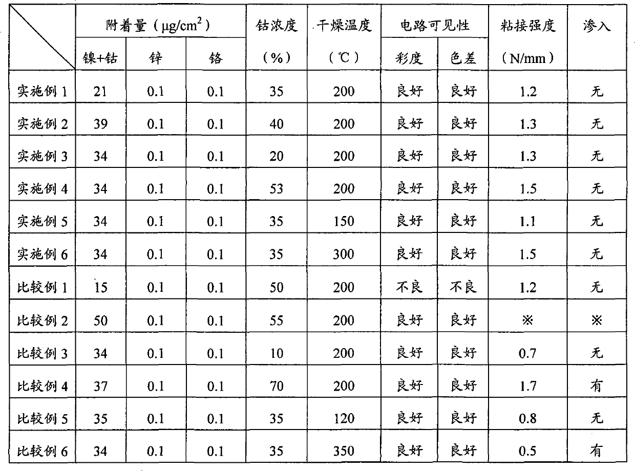
[0080] Using a rolled copper foil with a thickness of 16.3 μm as the original foil 1, in an aqueous solution of 40g / L sodium hydroxide and 20g / L sodium carbonate, set the temperature at 40°C and the current density at 5A / dm 2 1. Under the process condition of 10 seconds of processing time, electrolytic degreasing treatment is carried out through cathodic electrolysis process.

[0081] Next, at a temperature of 25° C., it was immersed in a 50 g / L sulfuric acid aqueous solution for 10 seconds to perform pickling treatment.

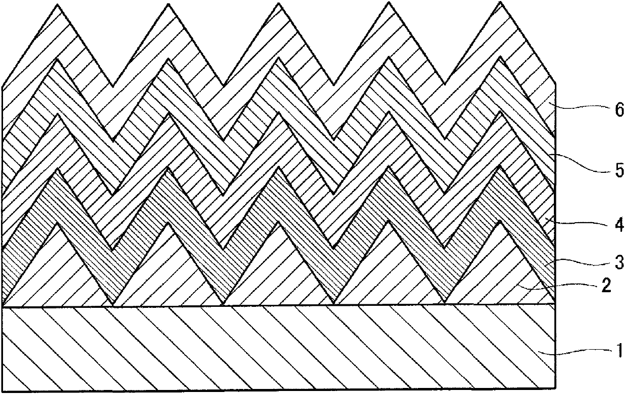
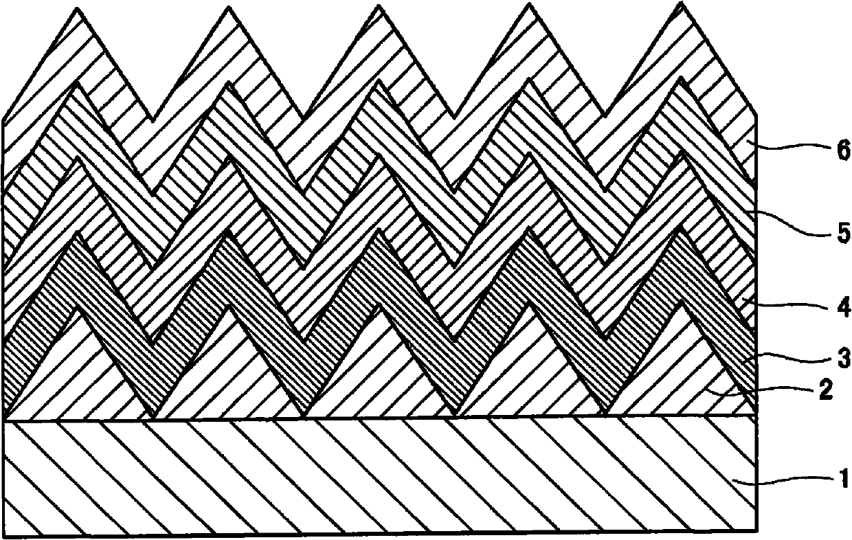
[0082] After roughening the original foil 1 to form the roughening plating layer 2, a nickel-cobalt alloy plating layer 3, a zinc plating layer 4, a chromium plating layer, and Salt treatment layer 5, silane coupling treatment layer 6.

[0083] More specifically, the nickel-cobalt alloy plating layer 3 is formed by a sulfuric acid bath, the zinc plating layer 4 is formed by a sulfuric acid bath after being prepared from a chemical, and the chromate treatmen...

Embodiment 2

[0093] In the sample related to this Example 2, the deposition amount of the nickel-cobalt alloy plating layer 3 was set to 39 μg / cm 2 , and the concentration of cobalt (Co) in the nickel-cobalt alloy plating layer 3 was set to 40% by mass. Then, other settings were the same as those of the sample according to Example 1.

[0094] It was confirmed that the sample according to this Example 2 was also good in all characteristics such as circuit visibility, adhesive strength, and penetration. In particular, the adhesive strength was 1.3 N / mm, which was somewhat improved compared to 1.2 N / mm in the case of Example 1.

Embodiment 3

[0096] In the sample related to this Example 3, the deposition amount of the nickel-cobalt alloy plating layer 3 was set to 34 μg / cm 2 , and the concentration of cobalt (Co) in the nickel-cobalt alloy plating layer 3 was set to 20% by mass. Then, other settings were the same as those of the sample according to Example 1.

[0097] It was confirmed that the sample according to this Example 3 was also good in all characteristics such as circuit visibility, adhesive strength, and penetration as in the case of Example 2.


PUM

PropertyMeasurementUnit
Thicknessaaaaaaaaaa
Adhesive strengthaaaaaaaaaa

Abstract

The present invention provides a copper foil for printed circuit boards and a method for manufacturing the same, the copper foil has high visibility of penetrating an insulating base material, and it is possible to avoid inleakage and peeling in a process of manufacturing the printed circuit board. The copper coil for the printed circuit board is characterized in that the copper coil is used for forming a conductor distribution picture of the printed circuit board and is pasted to the surface of the insulating base material, and has a cobalt-nickel alloy plating layer in which a chroma (based on Japanese Industrial Standard JIS Z 8729) c *= (a*2 + b*2) 1/2 of the surface of the copper coil is less than 6 optically detected by spacing the insulating base material.

Description

technical field [0001] The present invention relates to a method for forming various wiring patterns such as wiring patterns of a printed circuit board such as a tape carrier for a semiconductor device, which is bonded to the surface of an insulating base material formed of, for example, a polyimide resin film. A copper foil for a printed wiring board is particularly suitable for a printed wiring board or the like in which the position of the pattern is recognized by seeing through an insulating base material after the pattern is formed, and a method for producing the same. Background technique [0002] Conventionally, copper foils have been generally used as conductor layers for forming wiring patterns of printed circuit boards and various wiring patterns such as so-called inner lead parts. [0003] Especially in the field of flexible printed wiring boards, copper clad substrates for flexible printed wiring boards are formed by laminating copper foil with a thickness of sev...

Claims


Application Information

Patent Timeline
IPC IPC(8): H05K3/38H05K1/09
CPCB32B15/08B32B15/20B32B2457/08C23C28/321C23C28/34C23C2222/20H05K1/0346H05K2201/0154
Inventor 伊藤保之额贺恒次
Owner CHANG CHUN PETROCHEMICAL CO LTD
Why Eureka
Try Eureka