Method for preparing surface plasma resonance chip

A surface plasma and chip technology, applied in ion implantation plating, metal material coating process, coating, etc., to achieve the effect of uniform thickness, smooth surface and controllable thickness

Active Publication Date: 2011-04-06
JIANGXI INST OF RARE EARTHS CHINESE ACAD OF SCI
2 Cites 5 Cited by

AI-Extracted Technical Summary

Problems solved by technology

Dong Shaojun's group used the method of anode electrolysis to process the gold film with a thickness greater than 50nm to 50nm. This method is to electrolyze part of the gold film into...

Method used

As can be seen from above-mentioned technical scheme, the present invention provides a kind of preparation method of surface plasmon resonance chip, comprising: step a) glass substrate is put into the growth chamber of vacuum sputtering instrument; Introduce argon into the growth chamber, vacuumize to 10-1-10-3 mbr, use chromium as the target material, and the distance between the target and the base is 5-9 cm, and sputter a chromium film on the glass substrate; step c) use gold...

Abstract

The embodiment of the invention discloses a method for preparing a surface plasma resonance chip. The method comprises the following steps of: a) placing a glass substrate in a growth chamber of a vacuum sputtering instrument; b) introducing argon gas into the growth chamber, vacuuming until the vacuum degree is 10<-1> to 10<-3>mbr and sputtering a chromium thin film on the glass substrate at a substrate-to-target distance of 5 to 9cm by taking chromium as a target material; and c) sputtering a metal thin film on a product obtained in the step b) at the substrate-to-target distance of 5 to 9cm under the condition of vacuum degree of between 10<-1> and 10<-3>mbr by taking metal as the target material. By using a vacuum sputtering principle and the substrate-to-target distance of 5 to 9cm, the prepared metal thin film has a flat surface and controllable thickness and can be used for the surface plasma resonance chip. Experiment results show that the prepared metal thin film has uniform thickness which is about 50nm.

Application Domain

Technology Topic

ChromiumPlasma resonance +4

Image

  • Method for preparing surface plasma resonance chip
  • Method for preparing surface plasma resonance chip
  • Method for preparing surface plasma resonance chip

Examples

  • Experimental program(6)

Example Embodiment

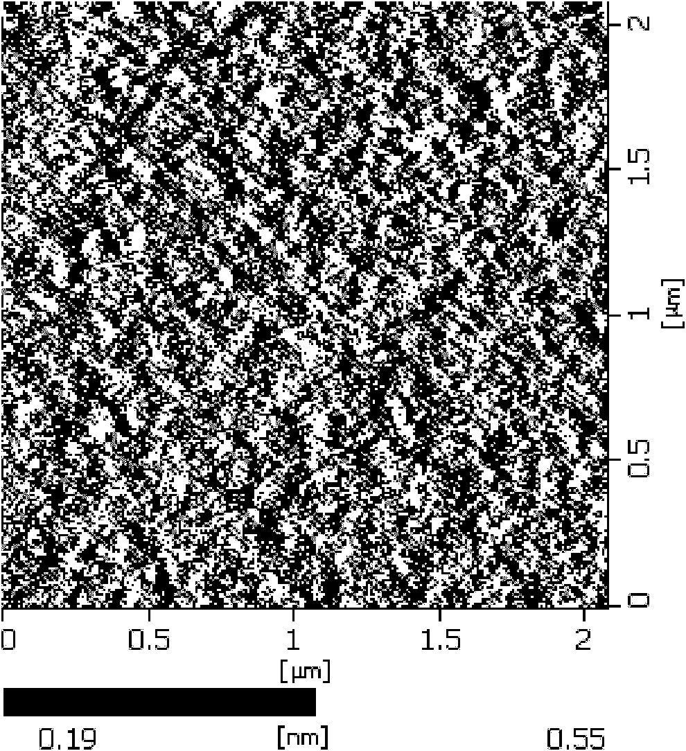
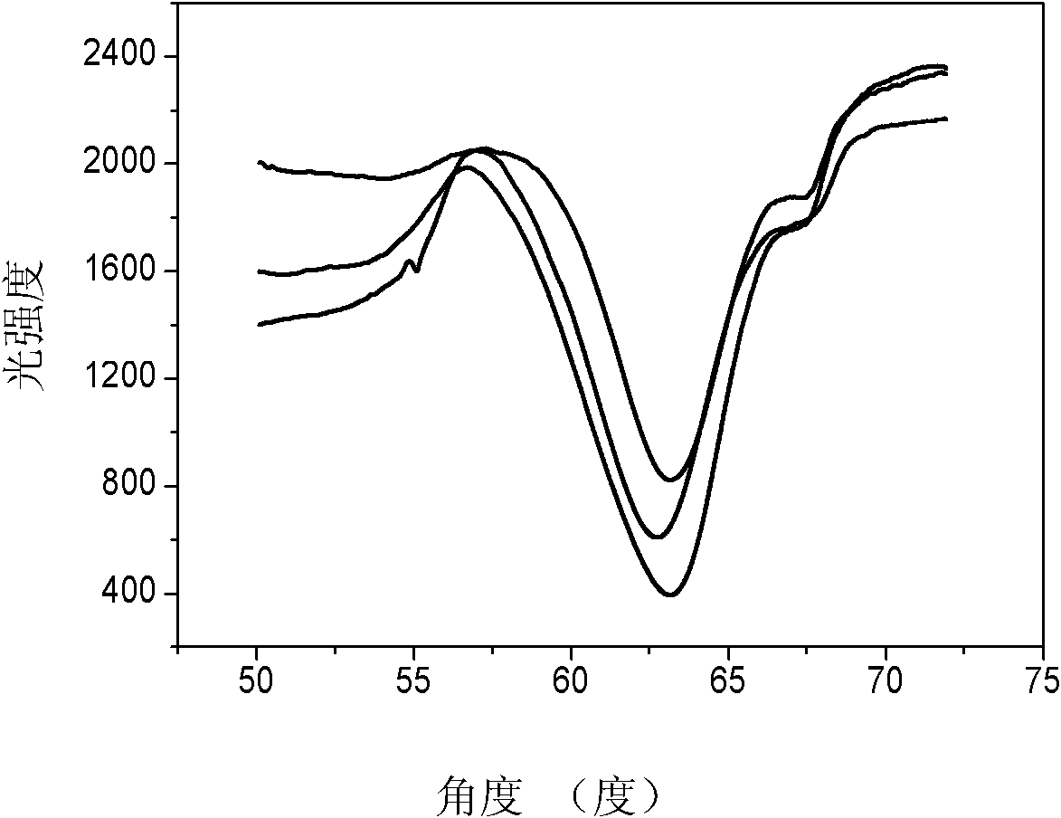
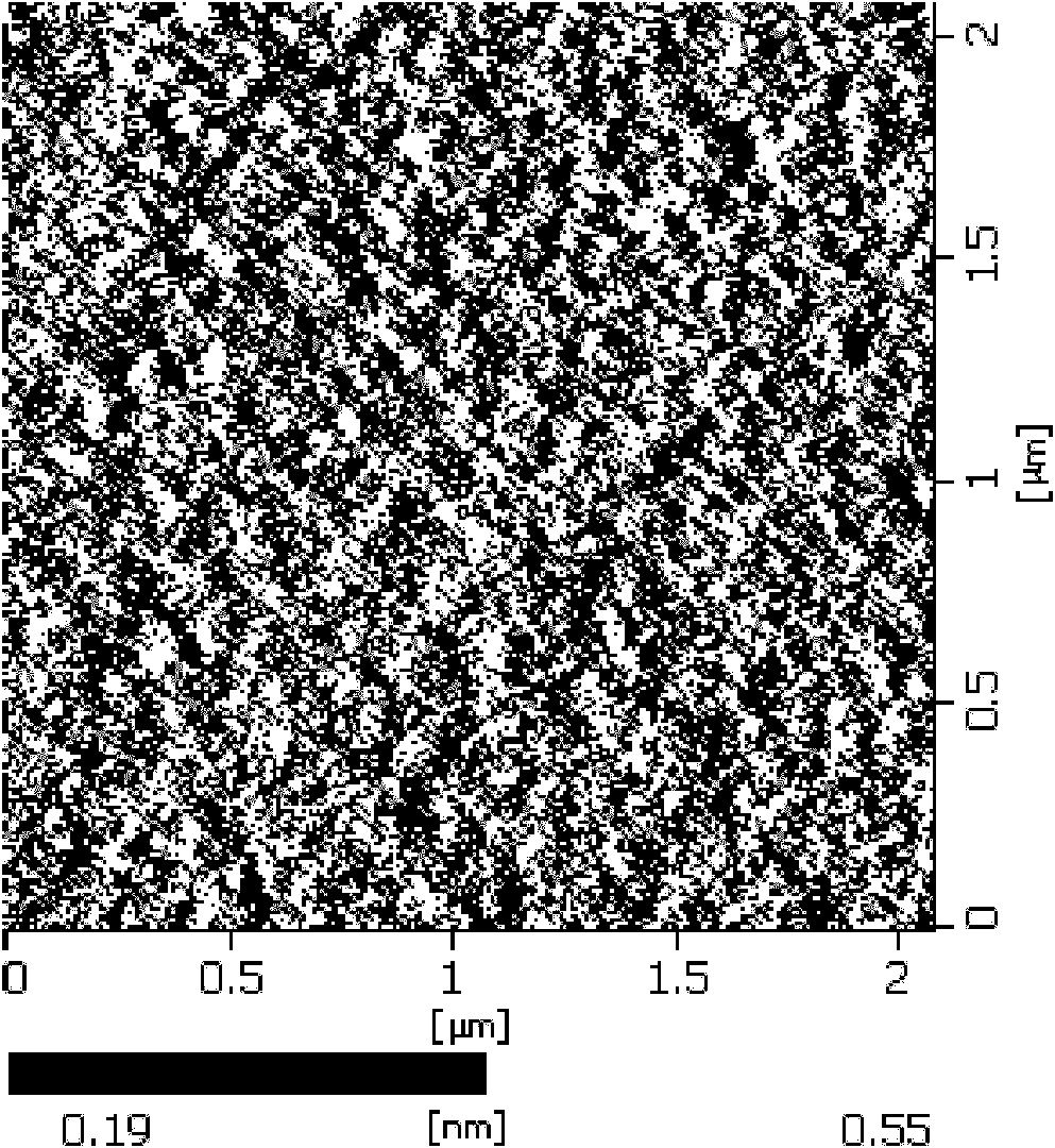
[0028] The invention discloses a method for preparing a surface plasmon resonance chip, including:
[0029] Step a) Put the glass substrate into the growth chamber of the vacuum sputtering apparatus;
[0030] Step b) Pour argon gas into the growth chamber and vacuumize to 10 -1 ~10 -3 mbr, using chromium as a target with a target base distance of 5-9 cm, and sputtering a chromium film on the glass substrate;
[0031] Step c) Pour argon gas into the growth chamber and vacuumize to 10 -1 ~10 -3 mbr, using gold as a target with a target base distance of 5-9 cm, and sputtering a gold film on the product obtained in step b).
[0032] According to the present invention, it preferably includes pretreatment of the glass substrate, preferably specifically:
[0033] Put the glass substrate in a volume ratio of 0.8~1.2:2.5~3.5 30wt% H 2 O 2 With 98wt% H 2 SO 4 The mixed solution is heated, then rinsed with water, dried by a nitrogen stream, the H 2 O 2 With H 2 SO 4 The volume ratio of is more preferably 0.9-1.1:2.8-3.2, most preferably 1:3.
[0034] The vacuum sputtering apparatus preferably adopts the SCD050 vacuum sputtering system of Germany BALZERS company.
[0035] In the step b), the sputtering current is preferably 110-130 mA, more preferably 120 mA. The sputtering time in the step b) is preferably 30-50 seconds, more preferably 40 seconds. The principle of vacuum sputtering in the present invention is that electrons are accelerated under the action of an electric field and collide with argon atoms in the process of flying to the glass substrate, ionizing a large number of argon ions and electrons, and the electrons fly to the glass substrate, and the argon ions are The electric field accelerates the bombardment of the target, sputtering out a large number of target atoms, and the neutral target atoms or molecules are deposited on the glass substrate to form a film.
[0036] In the step c), the sputtering current is preferably 50-70 mA, more preferably 60 mA. The sputtering time in the step c) is preferably 160 to 480 seconds. Said step c) is preferably:
[0037] Step c1) Pour argon gas into the growth chamber and evacuate to 10 -1 ~10 -3 mbr, using gold as a target with a target base distance of 5-9 cm, sputtering a gold film on the product obtained in step b) for 40-120 seconds, and cooling;
[0038] Step c2) Sputter a gold film on the product obtained in step c1) for 80 to 240 seconds, and cool;
[0039] Step c3) Sputtering a gold film on the product obtained in the step c1) for 120-360 seconds.
[0040] The step c1) preferably stays for 10-30 minutes after sputtering, and more preferably stays for 15-20 minutes. The step c2) preferably stays for 10-30 minutes after sputtering, and more preferably stays for 15-20 minutes. The present invention preferably adopts the above-mentioned intermittent sputtering method, so as to cool the gold target and ensure the uniformity of the plated gold film.

Example Embodiment

[0043] Example 1
[0044] Pretreatment of glass substrate:
[0045] Put a glass substrate with a size of 20×20mm in a volume ratio of 1:3 30wt% H 2 O 2 With 98wt% H 2 SO 4 Boil the mixed solution for 30 minutes, then rinse with water and blow dry with nitrogen flow;
[0046] Chrome film:
[0047] Adjust the target base distance of the SCD 050 vacuum sputtering system produced by Germany BALZERS to 5cm, and put the glass substrate dried by the nitrogen stream into the growth chamber of the vacuum sputtering system;
[0048] Rotate the tee connected to SCD 050 to the closed state, turn on the water cooling system, and indicate the temperature is 12 ~ 6 ℃; open the argon cylinder, rotate the tee of the gas supply system to communicate with SCD 050, and provide argon to the system;
[0049] Install the chromium target, turn the "shutter" of the vacuum sputtering system to the closed state, and the "shutter" is separated between the chromium target and the glass substrate;
[0050] Turn on the function version of the vacuum sputtering system, adjust it to the "sputtering" gear, and set the sputtering time to 50 seconds;
[0051] Press the "switch" button of the vacuum sputtering system to turn on the SCD 050, and press the "clean" button until the vacuum of the growth chamber of the vacuum sputtering system reaches 10 -2 mbar;
[0052] Press the "start sputtering" button, adjust the current value to 120mA, turn the "shutter" to the open state, and start sputtering;
[0053] After the sputtering is completed, turn the current button to the minimum and wait 15 minutes for the chromium target to cool down. The thickness of the chromium is about 5nm;
[0054] Gold-plated film:
[0055] Rotate the tee connected to the SCD 050 of the vacuum sputtering system to communicate with the outside, put in air until the internal and external pressures are equal, remove the chromium target, install the gold target, and turn the "shutter" to the closed state;
[0056] Reset the sputtering time to 120 seconds;
[0057] Turn on the "switch" button of the vacuum sputtering system and press the "clean" button until the vacuum reaches 10 -2 mbar;
[0058] Press the "Start Sputtering" button, adjust the current value to 60mA, turn the "Shutter" to the open state, and start sputtering;
[0059] After the sputtering is completed, turn the current button to the minimum, wait 15 minutes for the gold target to cool, and add the time button to 240 seconds;
[0060] Press the "sputtering start" button of the vacuum sputtering system, adjust the current value to 60mA, turn the "shutter" to the open state, and start sputtering. After the sputtering is complete, turn the current button to the minimum, and wait for 15 minutes to reach gold After the target is cooled, increase the time button to 360 seconds, then press the "sputter start" button to adjust the current value to 60mA, turn the "shutter" to the open state, and start sputtering. After the sputtering is complete, press the current button Rotate to the minimum, wait for 15 minutes to cool down the gold target, the thickness of the gold plating is 50nm;
[0061] Press the "switch" button to turn off the instrument, then unscrew the tee connected to the SCD 050 into the air, remove the gold target, and make a surface plasmon resonance chip;
[0062] Close the functional version, close the three-way connection with SCD 050, close the cooling water, and close the main valve of the argon cylinder.
[0063] Such as figure 1 As shown, this is an atomic force microscope picture of the surface plasmon resonance chip prepared in this embodiment. It can be seen from the figure that the surface of the gold film of the surface plasmon resonance chip prepared in the present invention is uniform.
[0064] Take the surface plasmon resonance chip prepared in Example 1, the surface plasmon resonance chip with a thickness of 40 nm and the surface plasmon resonance chip with a thickness of 60 nm, respectively, and place them in an aqueous solution for SPR peak shape detection, such as figure 2 Shown are the SPR peak shapes of the surface plasmon resonance chip, the surface plasmon resonance chip with a thickness of 40 nm, and the surface plasmon resonance chip with a thickness of 60 nm prepared in the embodiment of the present invention in an aqueous solution. The curves in the figure respectively correspond to the surface plasmon resonance chip with a thickness of 60 nm, the surface plasmon resonance chip with a thickness of 40 nm and the surface plasmon resonance chip with a thickness of 50 nm prepared in Example 1 from top to bottom. From figure 2 It can be seen that the surface plasmon resonance chip with a thickness of 50 nm prepared in Example 1 has a good response signal.

Example Embodiment

[0065] Example 2
[0066] Pretreatment of glass substrate:
[0067] Put a glass substrate with a size of 20×20mm in a volume ratio of 1:3 30wt% H 2 O 2 With 98wt% H 2 SO 4 Boil the mixed solution for 30 minutes, then rinse with water and blow dry with nitrogen flow;
[0068] Chrome film:
[0069] Adjust the target base distance of the SCD 050 vacuum sputtering system produced by German BALZERS to 6 cm, and put the glass substrate dried by the nitrogen stream into the growth chamber of the vacuum sputtering system;
[0070] Rotate the three-way connected with SCD 050 to the closed state, turn on the water cooling system, and indicate the temperature is 12-16 ℃; open the argon cylinder, rotate the three-way of the gas supply system to communicate with SCD 050, and provide argon to the system;
[0071] Install the chromium target, turn the "shutter" of the vacuum sputtering system to the closed state, and the "shutter" is separated between the chromium target and the glass substrate;
[0072] Turn on the function version of the vacuum sputtering system, adjust it to the "sputtering" file, and set the sputtering time to 45 seconds;
[0073] Press the "switch" button of the vacuum sputtering system to turn on the SCD 050, and press the "clean" button until the vacuum of the growth chamber of the vacuum sputtering system reaches 10 -2 mbar;
[0074] Press the "start sputtering" button, adjust the current value to 120mA, turn the "shutter" to the open state, and start sputtering;
[0075] After the sputtering is completed, turn the current button to the minimum and wait 15 minutes for the chromium target to cool down. The thickness of the chromium is about 5nm;
[0076] Gold-plated film:
[0077] Rotate the tee connected to the SCD 050 of the vacuum sputtering system to communicate with the outside, put in air until the internal and external pressures are equal, remove the chromium target, install the gold target, and turn the "shutter" to the closed state;
[0078] Reset the sputtering time to 100 seconds;
[0079] Turn on the "switch" button of the vacuum sputtering system and press the "clean" button until the vacuum reaches 10 -2 mbar;
[0080] Press the "Start Sputtering" button, adjust the current value to 60mA, turn the "Shutter" to the open state, and start sputtering;
[0081] After the sputtering is completed, turn the current button to the minimum, wait 15 minutes for the gold target to cool, and add the time button to 200 seconds;
[0082] Press the "sputtering start" button of the vacuum sputtering system, adjust the current value to 60mA, turn the "shutter" to the open state, and start sputtering. After the sputtering is complete, turn the current button to the minimum, and wait for 15 minutes to reach gold After the target is cooled, increase the time button to 300 seconds, press the "sputter start" button, adjust the current value to 60mA, turn the "shutter" to the open state, and start sputtering. After the sputtering is complete, press the current button Rotate to the minimum, wait for 15 minutes to cool down the gold target, the thickness of the gold plating is 50nm;
[0083] Press the "switch" button to turn off the instrument, then unscrew the tee connected to the SCD 050 into the air, remove the gold target, and make a surface plasmon resonance chip;
[0084] Close the functional version, close the three-way connection with SCD 050, close the cooling water, and close the main valve of the argon cylinder.

PUM

PropertyMeasurementUnit
Thickness40.0 ~ 60.0nm
tensileMPa
Particle sizePa
strength10

Description & Claims & Application Information

We can also present the details of the Description, Claims and Application information to help users get a comprehensive understanding of the technical details of the patent, such as background art, summary of invention, brief description of drawings, description of embodiments, and other original content. On the other hand, users can also determine the specific scope of protection of the technology through the list of claims; as well as understand the changes in the life cycle of the technology with the presentation of the patent timeline. Login to view more.

Similar technology patents

Classification and recommendation of technical efficacy words

  • Flat surface
  • Controllable thickness

Reinforced aerogel composite material and preparation method thereof

ActiveCN104496403AFlat surfaceGood flexural resistanceThermal insulationEnergy absorption
Owner:NANJING WEICAI NEW ENERGY TECH

Rapid preparation process of inert dispersion fuel pellet

ActiveCN106971764AGood sphericityControllable thicknessNuclear energy generationReactors manufacturePrillVolume fraction
Owner:MATERIAL INST OF CHINA ACADEMY OF ENG PHYSICS +1
Why Eureka
Try Eureka