Method for manufacturing semiconductor device

A manufacturing method and semiconductor technology, which can be used in semiconductor/solid-state device manufacturing, electrical components, radiation control devices, etc., and can solve the problem of large difference in thickness of the dielectric layer of the chip.

Inactive Publication Date: 2011-04-20
SEMICON MFG INT (SHANGHAI) CORP
View PDF0 Cites 11 Cited by
  • Summary
  • Abstract
  • Description
  • Claims
  • Application Information

AI Technical Summary

Problems solved by technology

[0011] The invention provides a method for manufacturing a semiconductor device to solve the defect that the thickness difference of the dielectric layer of the chip formed at the edge position and the center position of the wafer is relatively large in the existing semiconductor device manufacturing method

Method used


Image

  • Method for manufacturing semiconductor device
  • Method for manufacturing semiconductor device
  • Method for manufacturing semiconductor device

Examples


Embodiment Construction

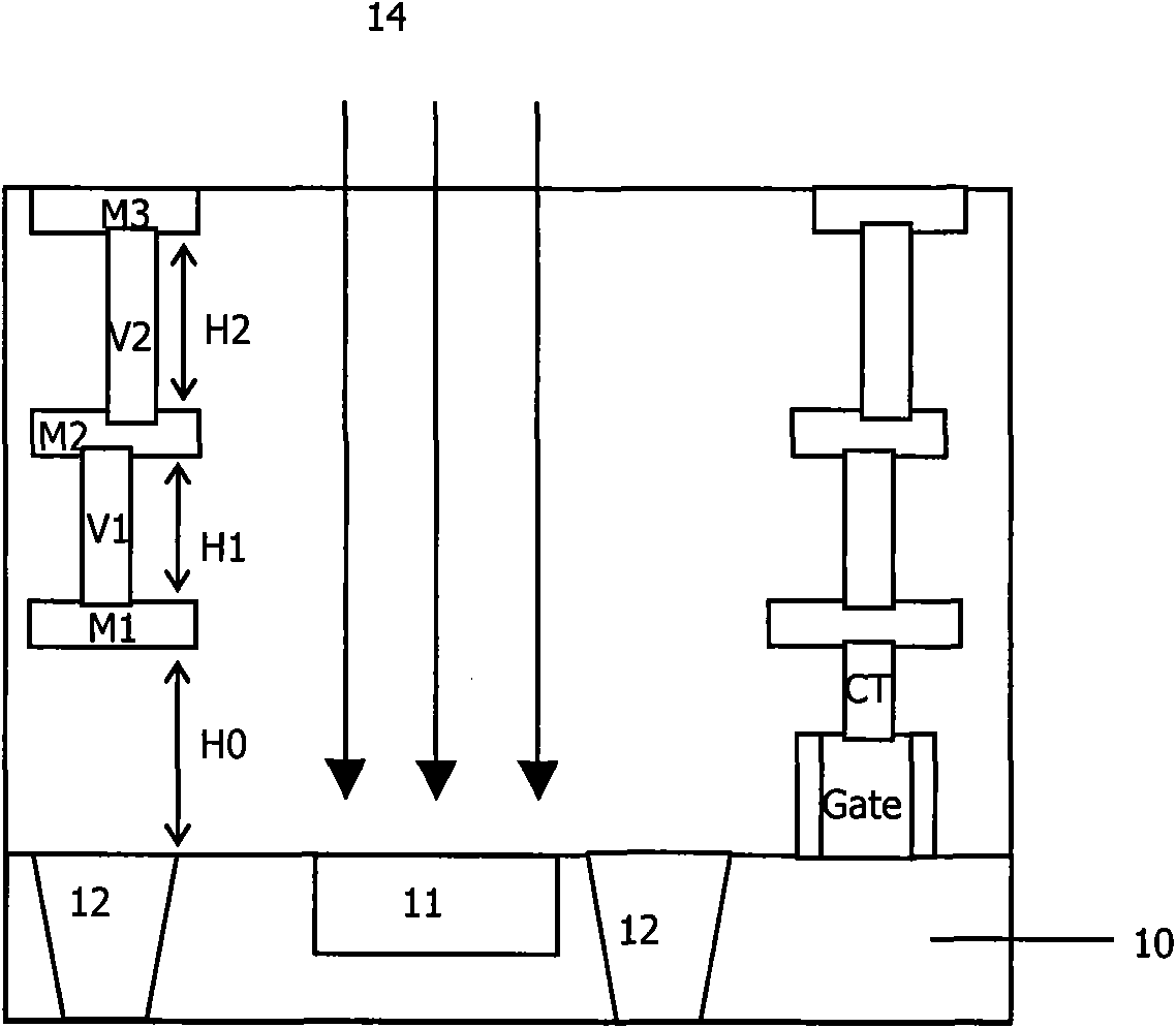
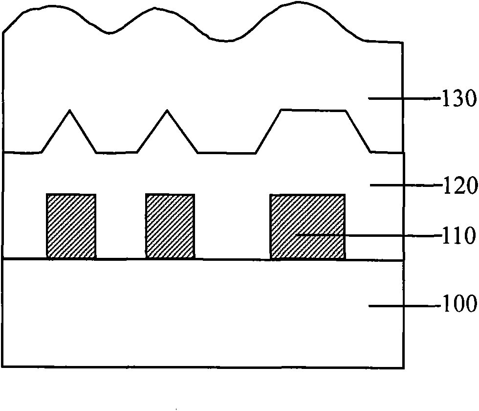
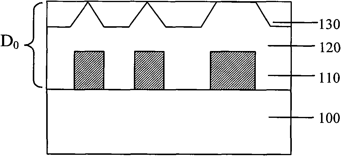
[0026] According to the background technology, the method for increasing the sensitivity of the CIS chip in the prior art is to use the CMP process to polish the dielectric layer of the wafer (including the interlayer dielectric layer ILD, the intermetal dielectric layer IMD, and the metal front dielectric layer PMD) , to reduce the thickness of the dielectric layer, but because the CMP process has different polishing rates for the center and the edge of the wafer, the method described on the wafer will cause the height difference between the center of the wafer and the surface of the edge of the wafer to be too high Large, resulting in a decline in the yield of the wafer. Therefore, the present invention proposes a method. After the dielectric layer is formed, an etching barrier layer is deposited on the dielectric layer, and then a DUO layer is formed on the dielectric layer by a spin coating process, and then the DUO layer is sequentially etched by an etching process. The e...


PUM


Abstract

The invention discloses a method for manufacturing a semiconductor device. The method comprises the following steps of: providing a semiconductor substrate, wherein a protrusion structure is arranged on the semiconductor substrate; depositing a first dielectric layer and an etching barrier layer on the semiconductor substrate in turn by adopting a deposition process, wherein upper surfaces of theetching barrier layer and the first dielectric layer at corresponding positions of the protrusion structure are higher than those at other positions; forming second dielectric layers with the same upper surface at different positions on the etching barrier layer by adopting a spin-coating process; etching the second dielectric layer to expose the highest point of the etching barrier layer by adopting a first etching process; and etching the second dielectric layer, the etching barrier layer and the first dielectric layer by adopting a second etching process until the etching barrier layer is completely removed. In the method, the thicknesses of the residual first dielectric layer at different positions on the whole wafer are the same, and the thickness of the first dielectric layer can bereduced. Therefore, the aim of improving the photosensitivity of the semiconductor device is fulfilled.

Description

technical field [0001] The invention relates to the field of semiconductor manufacturing, and in particular designs a method for manufacturing a semiconductor device. Background technique [0002] Complementary metal oxide semiconductor image sensor (CMOS image sensor, CIS) chip is a semiconductor device that converts optical signals into electrical signals. In recent years, due to many advantages in circuit integration, energy consumption and manufacturing cost, CIS has gained Rapid development. A high-performance CIS chip requires low dark current, a large dynamic operating range, and high sensitivity. [0003] The formula for calculating the sensitivity of the CIS chip is as follows: [0004] Sensitivity = voltage drop caused by incident photons / (incident light intensity * exposure time) [0005] Among them, the unit of sensitivity is mV / Lux*Second, and Lux ​​is the unit of incident light intensity. [0006] Reference attached figure 1 As shown, it is a schematic s...

Claims


Application Information

Patent Timeline
Patent Type & Authority Applications(China)
IPC IPC(8): H01L21/82H01L27/146
Inventor 邹立罗飞
Owner SEMICON MFG INT (SHANGHAI) CORP
Why Eureka
Try Eureka