Trench structure for power device and manufacturing method thereof

A technology of power devices and manufacturing methods, which is applied in the direction of semiconductor devices, electrical components, circuits, etc., can solve problems such as the influence of changes in silicon nitride films, deterioration of silicon oxide films, and changes in device performance, so as to meet the needs of high-quality, silicon Elimination of interface defects and good electrical properties

Inactive Publication Date: 2011-04-20
TIANJIN HUANXIN TECH DEV
View PDF6 Cites 25 Cited by
  • Summary
  • Abstract
  • Description
  • Claims
  • Application Information

AI Technical Summary

Problems solved by technology

The disadvantage of U.S. Patent No. 4,914,058 and U.S. No. 5,770,878 is that the silicon oxide film under the silicon nitride film is finally retained to maintain a thinner state than the bottom silicon oxide film. U.S. Patent No. 5,473,176 is formed by oxidation at the end The silicon oxide film under the original silicon nitride film is not removed even when the side wall is thin silicon oxide film
When dry etching the silicon nitride film on the bottom of the trench and the silicon wafer surface, the silicon oxide film under the silicon nitride film is prone to deterioration in the process, especially when the silicon nitride film is etched. When silicon oxide is exposed to a plasma environment, such deterioration tends to lead to increased leakage current between gate-source, or gate-emitter
The disadvantage of U.S. Patent No. 5,442,214 is that the silicon nitride film is still retained on the sidewall of the trench, which increases the threshold voltage of the device and the capacitance Cgs between the gate and the source, or the capacitance Cge between the gate and the emitter. In other words, these electrical parameters are not only affected by the fluctuation of the silicon oxide film, but also affected by the fluctuation of the silicon nitride film; at the same time, there is also the aforementioned degradation of silicon oxide under the silicon nitride film.
The disadvantage of U.S. Patent No. 5,473,176 is that, on the one hand, it is difficult to align the lower trench and the upper V-shaped structure, and it is easy to cause a difference in the thickness of the V-shaped insulating dielectric film on both sides due to the deviation on the overlay, so that the device On the other hand, after etching the silicon nitride film at the bottom of the lower trench, the method of continuing to etch the silicon oxide film by dry etching is easy to cause damage defects on the exposed silicon surface, and is easy to Subsequent high-temperature oxidation conditions grow into the device, resulting in device leakage

Method used


Image

  • Trench structure for power device and manufacturing method thereof
  • Trench structure for power device and manufacturing method thereof
  • Trench structure for power device and manufacturing method thereof

Examples


Embodiment Construction

[0032] The present invention will be further described below in conjunction with accompanying drawing and embodiment:

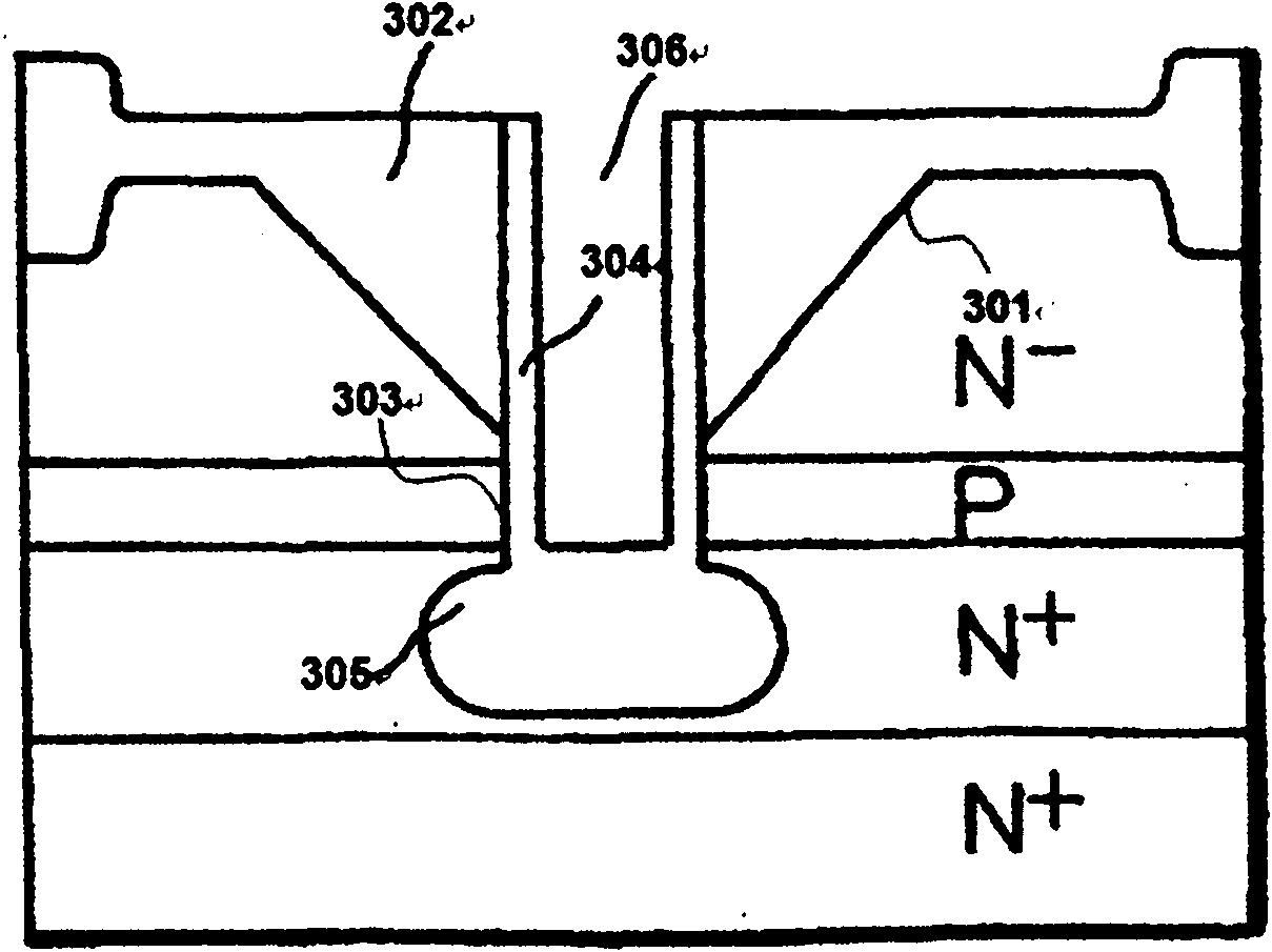
[0033] refer to Figure 5 The trench structure used for power devices is a trench (width: micron or submicron, Depth: 1-10 microns) 501 has a layer of selectively grown silicon oxide film 502 with a thick bottom and a high-quality silicon oxide film 503 with thin side walls, and the gap-free filling on the silicon oxide film 503 in the trench 501 has good electrical conductivity Doped polysilicon film 504, after the polysilicon film on the surface of the silicon wafer at the trench is removed, the surface of the silicon wafer forms a stepless or small step shape 505 within 1000 Angstroms. When removing the polysilicon film outside the trench, the silicon A layer of silicon oxide film 506 is left on the wafer surface to ensure that the silicon surface is not damaged.

[0034] The trench structure manufacturing method for power devices disclosed in the presen...


PUM


Abstract

The invention discloses a trench structure for a power device and a manufacturing method thereof. The trench structure has the characteristics that: a side wall is vertical and provided with a thin silicon oxide film or a side wall is provided with a slight slope (theta=80-90 degrees) and a thin silicon oxide film; the bottom is smooth and is provided with a thick silicon oxide film; doped polycrystals are filled without gaps; boundary defects are eliminated; and the surface of a wafer at a trench position does not have any step or has a small step. The manufacturing method for the trench structure comprises the following steps of: forming the trench through dry etching; removing surface defects of the trench by using an oxidation process; forming the side wall of the trench by using a silicon nitride film; and forming a silicon oxide film with a thick bottom and a thin side wall in the trench through selective oxidation, wet etching and reoxidation; filling a good-conductivity polysilicon film without gaps; and removing the excessive polysilicon film outside the trench through etching or a chemically mechanical polishing process to form the trench structure required by a trench type power device. The manufacturing method is simple and stable in process, and is easy to implement; and the manufactured device has the advantages of small area, good electrical characteristics and the like.

Description

technical field [0001] The invention relates to a structure and a manufacturing method of a power device, in particular to a trench structure for a power device and a manufacturing method thereof. Background technique [0002] In order to reduce the size of power devices and improve the performance of power devices, trench structures are introduced into power devices. Such as Trench Metal Oxide Semiconductor Field Effect Transistor (Trench MOSFET), Trench Insulated Gate Bipolar Transistor (Trench IGBT), Trench MOS Controlled Thyristor (Trench MCT) and similar devices. [0003] In terms of trench technology, whether it is applied to MOSFET devices, or applied to IGBT or other power devices, there have been many patents. Among the patents that realize the thickness of the insulating dielectric film at the bottom of the trench is thicker than that of the insulating dielectric film at the side wall of the trench, there are many patents that use silicon nitride film as sidewall ...

Claims


Application Information

Patent Timeline
Patent Type & Authority Applications(China)
IPC IPC(8): H01L29/423H01L21/28
Inventor 饶祖刚丛培金沈浩平冯春阳陆界江赵雁高景倩
Owner TIANJIN HUANXIN TECH DEV
Why Eureka
Try Eureka