Metal oxide semiconductor (MOS) field effect transistor (FET) structure and preparation method thereof

A technology of field effect transistors and semiconductors, applied in the direction of transistors, semiconductor/solid-state device manufacturing, electric solid-state devices, etc., can solve problems such as enlargement, difficulty in meeting requirements, and difficulty in achieving high-reliability hot-carrier injection, etc., to achieve Effects of reducing electric field strength, increasing process cost, and improving hot carrier injection (HCI) resistance

Active Publication Date: 2011-05-11
CSMC TECH FAB2 CO LTD
View PDF3 Cites 17 Cited by
  • Summary
  • Abstract
  • Description
  • Claims
  • Application Information

AI Technical Summary

Problems solved by technology

However, the method provided in this patent document is still to improve the hot carrier injection (HCI) by enlarging the junction depth of the lightly doped drain (LDD). This method is still difficult to meet when the carrier injection (HCI) requirements are increased
[0006] It can be seen that it is difficult for the existing techn

Method used


Image

  • Metal oxide semiconductor (MOS) field effect transistor (FET) structure and preparation method thereof
  • Metal oxide semiconductor (MOS) field effect transistor (FET) structure and preparation method thereof
  • Metal oxide semiconductor (MOS) field effect transistor (FET) structure and preparation method thereof

Examples


Embodiment Construction

[0039] In order to make the object, technical solution and advantages of the present invention clearer, the present invention will be further described in detail below in conjunction with the accompanying drawings.

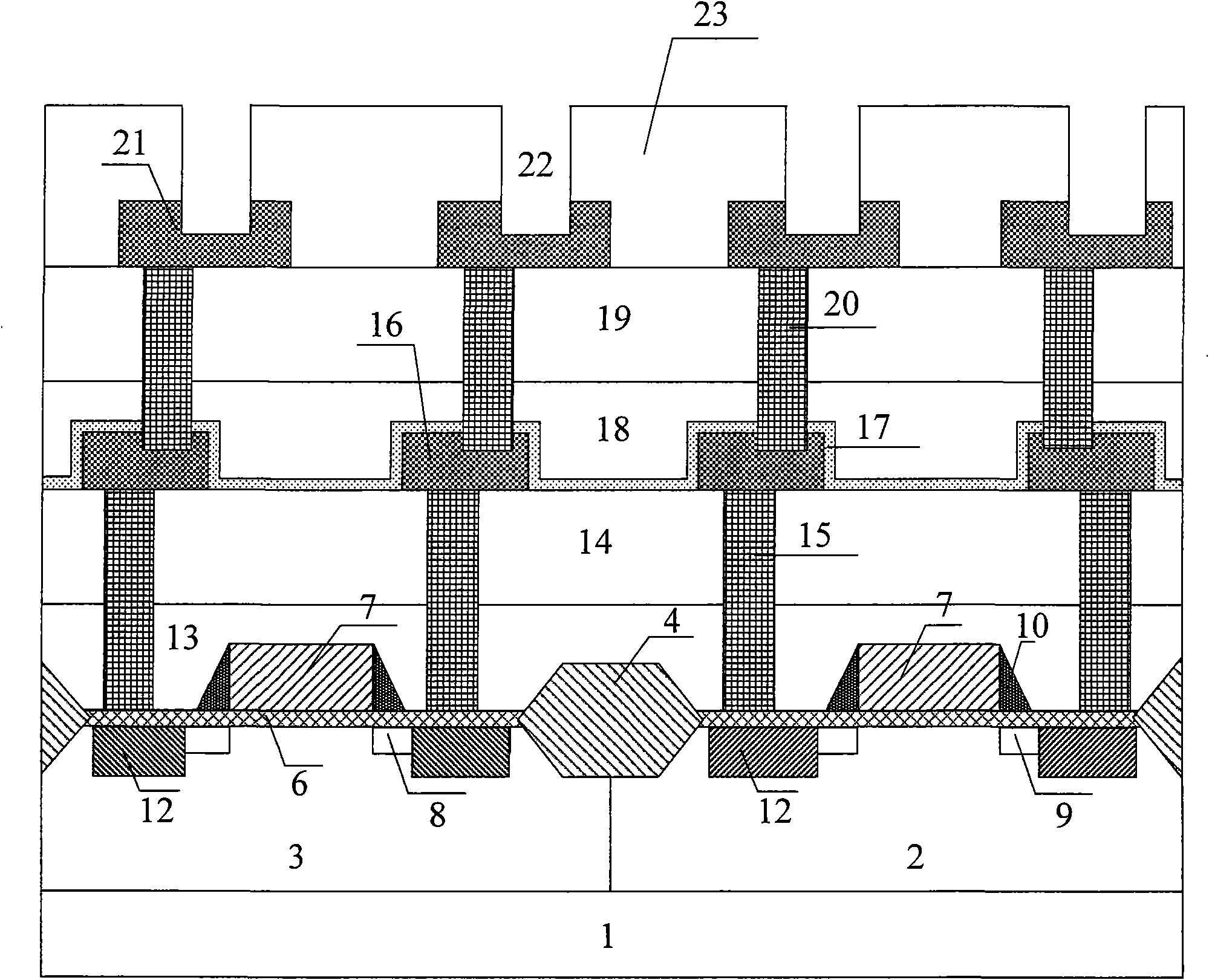
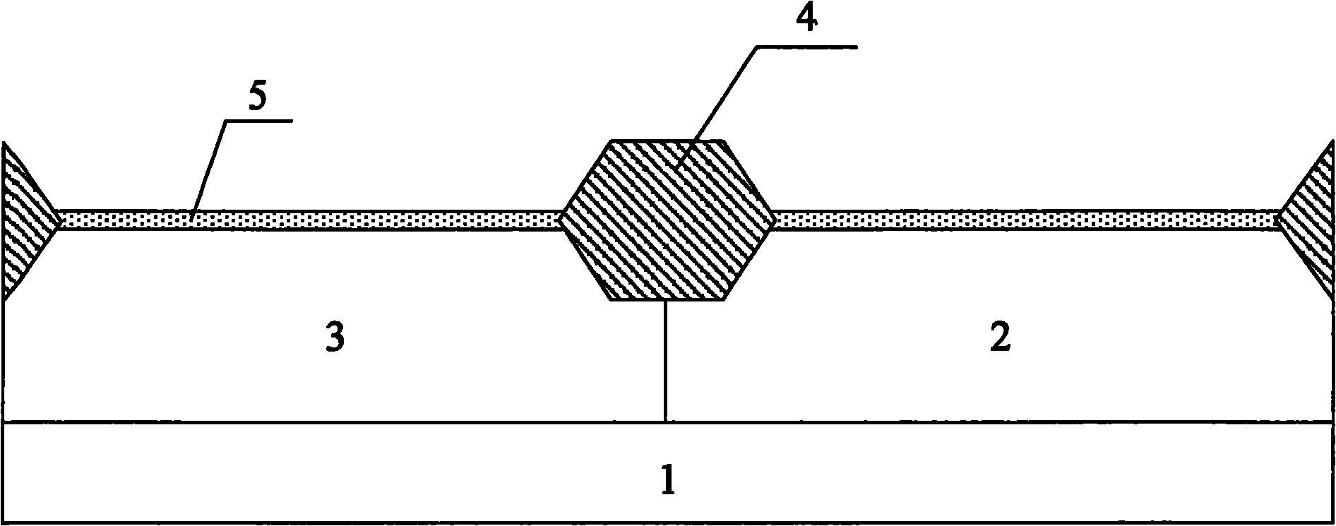
[0040] figure 1 It is a schematic diagram of a specific embodiment of the structure of a MOS field effect transistor provided by the present invention.

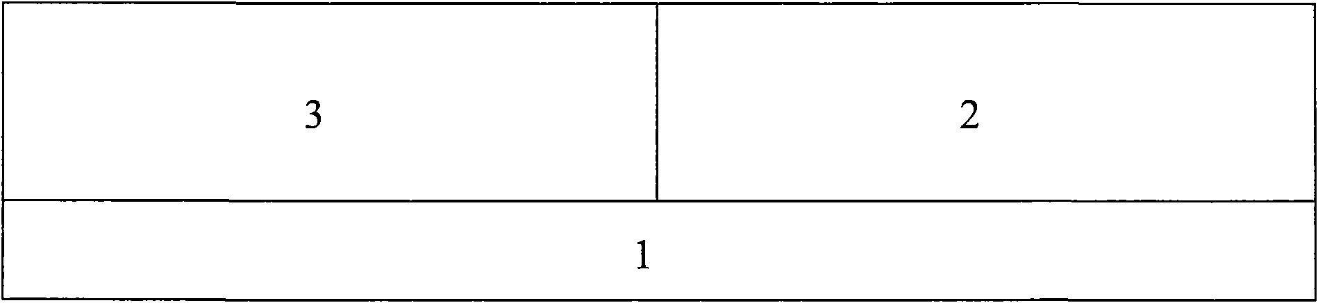
[0041] Such as figure 1 As shown, on the oriented P-type silicon substrate 1, there are N well region 2 and P well region 3, and there is a layer of gate oxide 6 on the upper surface of N well region 2 and P well region 3. , a polysilicon gate 7 is deposited on the gate oxide 6, and a layer of spacer (Spacer) 10 is deposited on the sidewall of the polysilicon gate 7, which is used to define the diffusion region of the lightly doped drain (LDD) structure, thereby avoiding short channels effect, the side wall (Spacer) 10 is orthoethyl silicate (TEOS). In addition, there is a field oxidation region 4 on the surf...


PUM


Abstract

The invention provides a metal oxide semiconductor (MOS) field effect transistor (FET) structure and a preparation method thereof. The MOSFET structure is used for improving reliability of hot carrier injection. In an MOS component structure and a preparation process thereof, lightly doped leak injection with a wide angle and a middle dose is adopted to reduce the probability of the hot carrier injection; a first metal layer is etched to form a metal interconnect metallic line, and then silicon-enriched silicon dioxide is used to replace traditional common silicon dioxide, so that the redundant dangling bonds of the Si in the layer are used for combining Si with other atoms (such as H), thus Si in a channel is combined with other atoms (such as N) to form firmer bonds so as to resist impact of carriers, maximally improve transconductance service life of the MOS component, improve the reliability of the hot carrier injection, and ensure current driving capacity of the MOS component; and meanwhile, in the preparation method of the MOSFET structure provided by the invention, conventional processes are utilized, thus having good process latitude and enhancing product yield to a certain extent.

Description

technical field [0001] The invention relates to the reliability of semiconductor devices, in particular to the improvement of the reliability of hot carrier injection of MOS devices, and belongs to the semiconductor processing technology. Background technique [0002] According to Moore's law and the principle of proportional reduction, with the increasing scale of semiconductor integrated circuits, the feature size of metal-oxide-semiconductor field-effect transistors (MOSFETs) has become smaller and smaller, and has now shrunk to submicron and deep submicron micron range. In order to be compatible with other circuits, the power supply voltage cannot be reduced proportionally with the size of the device. Therefore, the electric field strength in the lateral direction (channel direction) and vertical direction (vertical channel direction) of the device will be significantly enhanced. Under the action of a strong electric field, the energy of the carriers will be greatly inc...

Claims


Application Information

Patent Timeline
IPC IPC(8): H01L27/088H01L23/522H01L21/8234H01L21/336H01L21/265H01L21/768
CPCH01L2924/0002H01L2924/00
Inventor 胡金节李月影赵英翰陈正培吴孝嘉
Owner CSMC TECH FAB2 CO LTD
Why Eureka
Try Eureka