Semiconductor chip set

A semiconductor and chip set technology, applied in the field of semiconductor chip sets and their manufacturing, and high-power semiconductor components, can solve the problems of limited routing capability, excessive volume, and limited heat dissipation effect.

Inactive Publication Date: 2011-06-22
BRIDGE SEMICON
View PDF5 Cites 6 Cited by
  • Summary
  • Abstract
  • Description
  • Claims
  • Application Information

AI Technical Summary

Problems solved by technology

Thereby, the heat energy generated by the chip can be transferred to the substrate through the protruding part, and then reach a heat sink; however, the electrical contacts are not easy to be arranged on the insulating layer, and it is difficult to electrically connect with the next layer assembly, and Cannot provide multi-layer routing
[0019] Significant disadvantages of known packages and thermal pads
For example, electrical insulating materials with low thermal conductivity, such as epoxy resins, limit heat dissipation; however, electrical insulating materials with higher thermal conductivity, such as epoxy resins filled with ceramic or silicon carbide, have low adhesion and Due to the high cost of mass production, the electrical insulating material may delaminate due to heat during the production process or in the early stage of operation
If the substrate is a single-layer ci

Method used


Image

  • Semiconductor chip set
  • Semiconductor chip set
  • Semiconductor chip set

Examples


Embodiment Construction

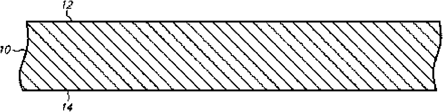
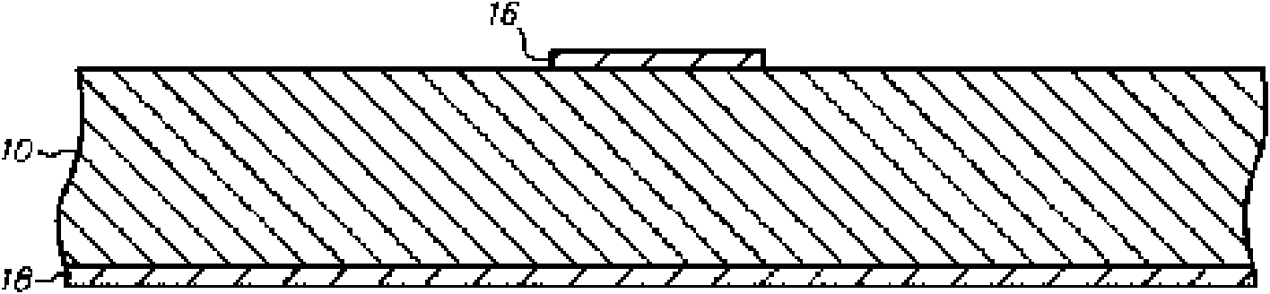
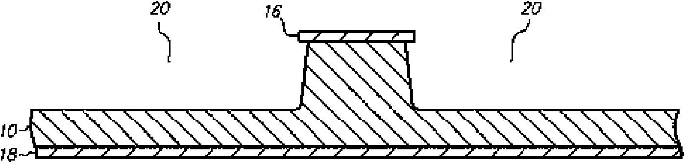
[0110] The invention is a semiconductor chip assembly body, which at least includes a semiconductor component, a heat dissipation seat, a substrate and an adhesive layer. The semiconductor component is electrically connected to the substrate and thermally connected to the heat dissipation seat, and the heat dissipation seat at least includes a protrusion and a base. wherein the protrusion extends upward through an opening of the adhesive layer and enters a through hole of the substrate, the base extends laterally from the protrusion, and the adhesive layer extends between the protrusion and the substrate and between the base and the substrate. The substrate at least includes first and second conductive layers and a dielectric layer therebetween. Thereby, the substrate can provide a pad and a terminal on the first conductive layer by using a routing line on the second conductive layer and the first and second conductive holes passing through the dielectric layer between the co...


PUM


Abstract

The invention relates to a semiconductor chip set at least comprising a semiconductor assembly, a heat-radiating seat, a base plate and an adhering layer, wherein the semiconductor assembly is electrically connected with the base plate and thermally connected with the heat-radiating seat; the heat-radiating seat at least comprises a protruding column and a base, wherein the protruding column upwards extends to pass through an opening of the adhering layer and enter a through hole of the base plate, and the base extends out of the side direction of the protruding column; the adhering layer extends between the protruding column and the base plate and between the base and the base plate; and the base plate at least comprises a first conducting layer, a second conducting layer and a dielectric layer and supplies a horizontal signal route between a weld pad positioned on the first conducting layer and a terminal, wherein the dielectric layer is positioned between the first conducting layerand the second conducting layer. The semiconductor chip set has high reliability and moderate price and is greatly suitable for quantity production and especially suitable for a high-power semiconductor chip set which is easy to generate high heat and needs excellent heat-radiating effect.

Description

Technical field: [0001] The invention relates to a semiconductor chip assembly body, in particular to a semiconductor chip assembly body which is suitable for high-power semiconductor components, especially a semiconductor chip assembly body composed of a semiconductor component, a substrate, an adhesive layer and a heat sink, and a manufacturing method thereof. Background technique: [0002] Semiconductor components such as packaged and unpackaged semiconductor chips can provide high voltage, high frequency and high performance applications; these applications perform specific functions, so the power consumption required is very high, but the higher the power, the semiconductor components The more heat produced. In addition, after the packaging density is increased and the size is reduced, the surface area available for heat dissipation is also reduced, resulting in increased heat generation. [0003] Semiconductor components are prone to problems such as performance degra...

Claims


Application Information

Patent Timeline
IPC IPC(8): H01L33/48H01L33/62H01L33/64
CPCH01L2224/45144H01L2224/48091H01L2224/49171H01L2924/181
Inventor 林文强王家忠
Owner BRIDGE SEMICON
Why Eureka
Try Eureka