Coarsening and etching method of large-area controllable surface of SiC substrate light emitting diode (LED) based on laser

A surface roughening and laser technology, which is applied in the direction of semiconductor devices, electrical components, circuits, etc., can solve the problems of long roughening etching time, high cost of etching equipment purchase and use, and reduced electrical performance of LEDs, etc., to achieve roughening The effects of flexible and diverse rough etching patterns, low cost of equipment and use, and improved current injection efficiency

Inactive Publication Date: 2011-06-29
SHANDONG UNIV
View PDF5 Cites 6 Cited by
  • Summary
  • Abstract
  • Description
  • Claims
  • Application Information

AI Technical Summary

Problems solved by technology

The disadvantages of using etching to roughen the light-emitting surface of LEDs are: (1) etching is very destructive to the carrier transport properties of semiconductor materials, which significantly reduces the electrical properties of LEDs; (2) ) The cost of purchasing and using etching equipment is extremely high, which greatly increases the cost of LEDs; (3) There is no way to control and optimize the shape and size of the roughened LED light-emitting surface by etching
(4) The roughening etching time is longer and the production efficiency is lower
The disadvantages of using chemical corrosion to roughen the light-emitting surface of LEDs are: (1) it is difficult to accurately control the rate and depth of corrosion, which is determined by the inherent defects of chemical methods; (2) it is susceptible to external environmental temperature and other factors impact, it is difficult to obtain highly repeatable roughened LED chips; (3) the structure obtained by etching is single, and it is difficult to optimize the light extraction effect
(4) The roughening etching time is longer and the production efficiency is lower
This method has high requirements for the epitaxial growth of semiconductor materials, is not easy to realize, and is extremely difficult to control
[0011] To sum up, the above technologies and patents do not have the characteristics of high controllability, low cost, easy combination with existing LED technology, non-toxicity, and no damage to the electrical properties of LED chips, and do not involve the laser-based highlight provided by the present invention. LED surface roughening method with extraction efficiency, high controllability, low cost, large area, various shapes, non-toxic, and no damage to LED chips

Method used


Image

  • Coarsening and etching method of large-area controllable surface of SiC substrate light emitting diode (LED) based on laser
  • Coarsening and etching method of large-area controllable surface of SiC substrate light emitting diode (LED) based on laser
  • Coarsening and etching method of large-area controllable surface of SiC substrate light emitting diode (LED) based on laser

Examples


Embodiment 1

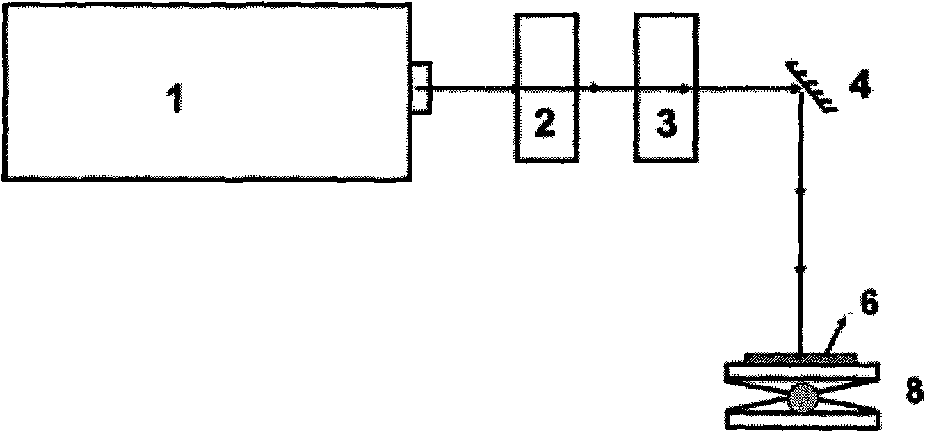
[0036] Taking a GaN-based front-mount LED epitaxial wafer on a 2-inch SiC substrate as an example to illustrate the implementation method of the present invention, the steps are as follows:

[0037] (1) The structure of GaN-based positive LED epitaxial wafers from bottom to top is SiC substrate, buffer layer GaN, intrinsic GaN layer, n-GaN confinement layer, multi-quantum well active light-emitting region, p-GaN confinement layer.

[0038] (2) Rough etching is performed on the p-GaN confinement layer, and the thickness of the p-GaN confinement layer is about 200 nm.

[0039] (3) Turn on the ultraviolet 355nm laser so that its laser output is in a standby state.

[0040] (4) Adjust the laser beam shaping module to obtain the beam energy distribution required for rough etching.

[0041] (5) Fix the GaN-based front-loading LED epitaxial wafer at the center of the lifting sample stage, adjust the lifting sample stage so that the ultraviolet 355nm laser beam is located in the cent...

Embodiment 2

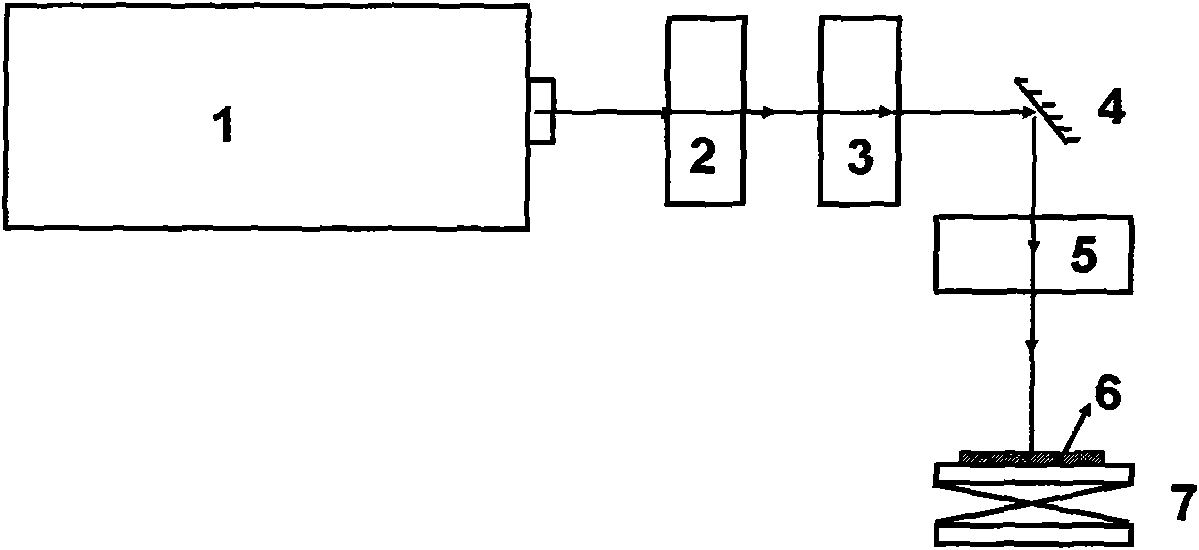
[0048] Take the 2-inch SiC substrate GaN-based vertical process LED epitaxial wafer as an example to illustrate the realization method of the present invention, the steps (4), (5), (9), and (10) are the same as those in Embodiment 1, the difference is:

[0049] (1) The structure of the GaN-based vertical process LED epitaxial wafer from bottom to top is SiC substrate, p-GaN confinement layer, multi-quantum well active light-emitting region, n-GaN confinement layer, and intrinsic GaN layer.

[0050] (2) Rough etching is performed on the intrinsic GaN layer, and the thickness of the intrinsic GaN layer is about 1.5 microns.

[0051] (3) Turn on the ultraviolet 355nm laser so that its laser output is in a standby state.

[0052] (6) Import the required roughening etching pattern into the high-precision electric displacement stage control software, for example, the vertical and horizontal stripe structure with a period of 15 microns, the roughening etching duty cycle is 50%, and t...

Embodiment 3

[0056] The implementation method of the present invention is illustrated by taking a 2-inch SiC substrate GaN-based LED epitaxial wafer as an example, and the steps (4), (5), (9), and (10) are the same as in Embodiment 1, the difference is that:

[0057] (1) The structure of the LED epitaxial wafer from the bottom to the top is the SiC substrate, the n-GaN confinement layer, the multi-quantum well active light-emitting region, and the p-GaN confinement layer.

[0058] (2) Perform roughening and roughening etching on the SiC substrate layer.

[0059] (3) Turn on the 355nm laser so that its laser output is in a standby state.

[0060] (6) Import the required roughening etching pattern into the high-speed galvanometer control software, for example, a concentric ring structure with an inner and outer layer interval of 20 microns, a roughening etching duty cycle of 50%, and a roughening etching area To cover the entire 2-inch SiC substrate.

[0061] (7) Control the output power o...


PUM


Abstract

The invention provides a coarsening and etching method of a large-area controllable surface of a SiC substrate light emitting diode (LED) based on a laser, belonging to the technical field of LED. The surfaces of the SiC substrate and an LED semiconductor material can be coarsened by utilizing that the semiconductor material highly absorbs high-power laser with a wavelength smaller than the absorption wavelength of the band edge of the semiconductor material to perform gasification. An area and a pattern coarsened and etched by the laser are controlled by a high speed scanner or a precise displacement stage; and the wire width and depth of coarsening and etching are regulated by controlling power and focusing degree of the laser. The method can be applied to coarsening and etching of the surface of the SiC substrate GaN-based LED with various structures. The laser is selected on the basis that the wavelength of the laser is smaller than the absorption wavelength of the band edge of the coarsened and etched semiconductor. The method has the advantages of wide application materials, high coarsening and etching speed, large coarsening and etching area, low cost, good coarsening effect, small damage on the semiconductor material and high controllability of coarsening and etching parameters of the system; and by using the method, the problem of coarsening the p-GaN layer and the SiC substrate can be effectively solved. Thus, the method has a great application potential in high-brightness LED production.

Description

Technical field: [0001] The invention relates to a laser-based large-area controllable surface roughening and etching method for SiC substrate LEDs, belonging to the technical field of light-emitting diode manufacturing. Background technique: [0002] In the 1950s, with the efforts of many well-known research institutions represented by IBM Thomas J. Watson Research Center, III-V semiconductors represented by GaAs rose rapidly in the field of semiconductor light emitting. Later, with the emergence of metal oxide chemical vapor deposition (MOCVD) technology, the growth of high-quality III-V semiconductors broke through the technical barrier, and semiconductor light-emitting diode devices with various wavelengths flooded into the market one after another. Compared with the current light-emitting devices, semiconductor light-emitting diodes have the characteristics of high theoretical efficiency, long life, and mechanical shock resistance, and are regarded as a new generation o...

Claims


Application Information

Patent Timeline
Patent Type & Authority Applications(China)
IPC IPC(8): H01L33/00
Inventor 左致远刘铎徐现刚何京良
Owner SHANDONG UNIV
Why Eureka
Try Eureka