

Organic light emitting device and preparation method thereof
A device and electroluminescence technology, applied in semiconductor/solid-state device manufacturing, electric solid-state devices, semiconductor devices, etc., can solve the problems of difficult process operation, serious concentration quenching effect, unbalanced carrier injection, etc., and achieve simplification Device structure and fabrication process, reduction of concentration quenching effect, effect of low turn-on voltage
- Summary
- Abstract
- Description
- Claims
- Application Information
AI Technical Summary
Problems solved by technology
Method used
Image

Examples
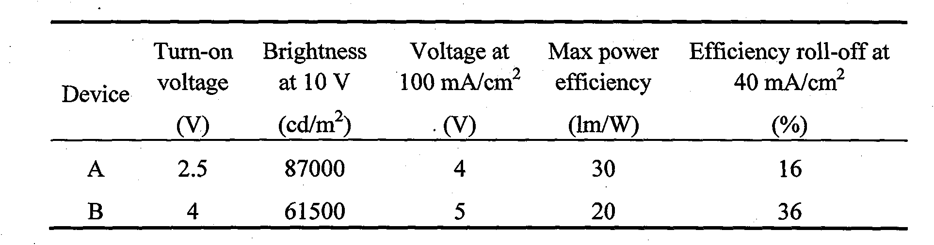
Embodiment 1
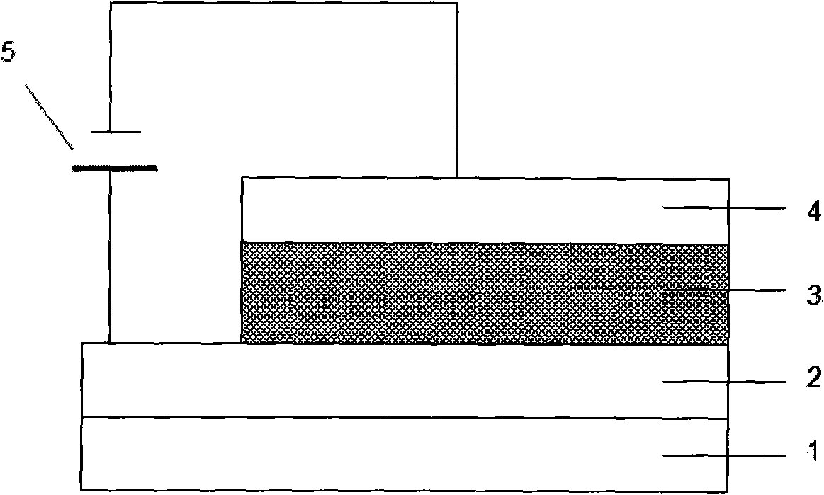
[0058] Such as figure 1 As shown, the functional layer 3 in the device structure includes a double host material of a hole transport material and an electron transport material.
[0059] The hole transport material of the device is NPB, and the electron transport material is Alq 3 , the cathode layer is Mg:Ag alloy. The entire device structure is described as:
[0060] Glass substrate / ITO / NPB:Alq 3 (100nm) / Mg:Ag(200nm)
[0061] The preparation method is as follows:
[0062] ①Use detergent, ethanol solution and deionized water to ultrasonically clean the transparent conductive substrate ITO glass, and dry it with dry nitrogen after cleaning. Wherein the ITO film on the glass substrate is used as the anode layer of the device, the square resistance of the ITO film is 10Ω / sq, and the film thickness is 180nm.
[0063] ② Move the dried substrate into a vacuum chamber, and pretreat the ITO glass with low-energy oxygen plasma for 10 minutes under an oxygen pressure environment ...
Embodiment 2
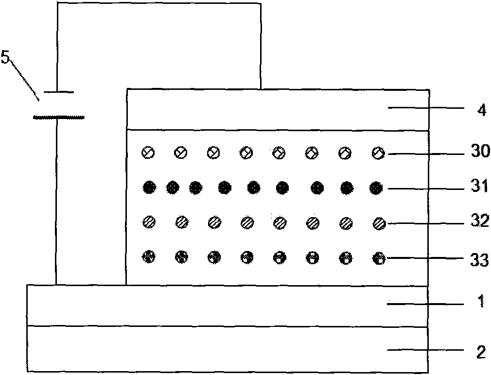
[0071] Such as figure 2 As shown, the functional layer 30 in the device structure includes a double host material of a hole transport material and an electron transport material, and the doped dye is a yellow phosphorescent dye.
[0072] The hole transport material of the device is TCTA, the electron transport material is Bphen, and the doping dye is (tbt) 2 Ir(acac), Mg:Ag alloy is used for the cathode layer. The entire device structure is described as:
[0073] Glass substrate / ITO / TCTA:Bphen:4%(tbt) 2 Ir(acac)(100nm) / Mg:Ag(200nm)
[0074] The preparation process of device A is similar to that of Example 1, wherein the evaporation rate of the organic material in step ③ is:
[0075] The gradient of the evaporation rate of the hole transport material decreases gradually: 1nm / s→0nm / s;
[0076] The gradient of the evaporation rate of the electron transport material is gradually increased: 0nm / s→1nm / s;
[0077] The evaporation rate of the yellow phosphorescent dye is mainta...
Embodiment 3
[0083] Such as figure 2 As shown, the functional layer 31 in the device structure includes a double host material of a hole transport material and an electron transport material, and the doped dye is a red fluorescent dye.
[0084] The hole transport material of the device is TCTA, the electron transport material is Bphen, the doping dye is DCJTB, and the cathode layer is Mg:Ag alloy. The entire device structure is described as:
[0085] Glass substrate / ITO / TCTA:Bphen:1%DCJTB(100nm) / Mg:Ag(200nm)
[0086] The preparation process of the device is similar to that of Example 1, wherein the evaporation rate of the organic material in step ③ is:
[0087] The gradient of the evaporation rate of the hole transport material decreases gradually: 1nm / s→0nm / s;
[0088] The gradient of the evaporation rate of the electron transport material is gradually increased: 0nm / s→1nm / s;
[0089] The evaporation rate of the red fluorescent dye is maintained at 0.001nm / s.
PUM
| Property | Measurement | Unit |
|---|---|---|
| luminous efficiency | aaaaa | aaaaa |
| thickness | aaaaa | aaaaa |
Abstract
Description
Claims
Application Information