Preparation method of single crystal cubic carbon nitride thin film
A technology of cubic carbon nitride and thin film, applied in chemical instruments and methods, single crystal growth, single crystal growth, etc., can solve the problem of not preparing single crystal cubic structure, achieve complete structure, high conversion rate, Simple operation effect
- Summary
- Abstract
- Description
- Claims
- Application Information
AI Technical Summary
Problems solved by technology
Method used
Image
Examples
Embodiment 1
[0030] A method for preparing a single crystal cubic carbon nitride film, comprising the steps of:
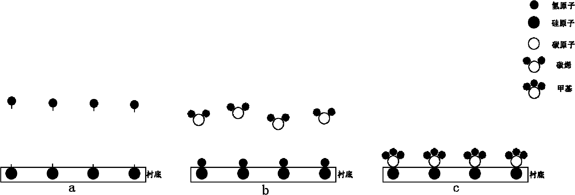
[0031] Step 101, under plasma conditions at 200°C, treat the surface of the silicon (111) substrate with hydrogen for 5 minutes to form Si-H bonds on the surface of the silicon substrate, such as figure 1 As shown in figure a;
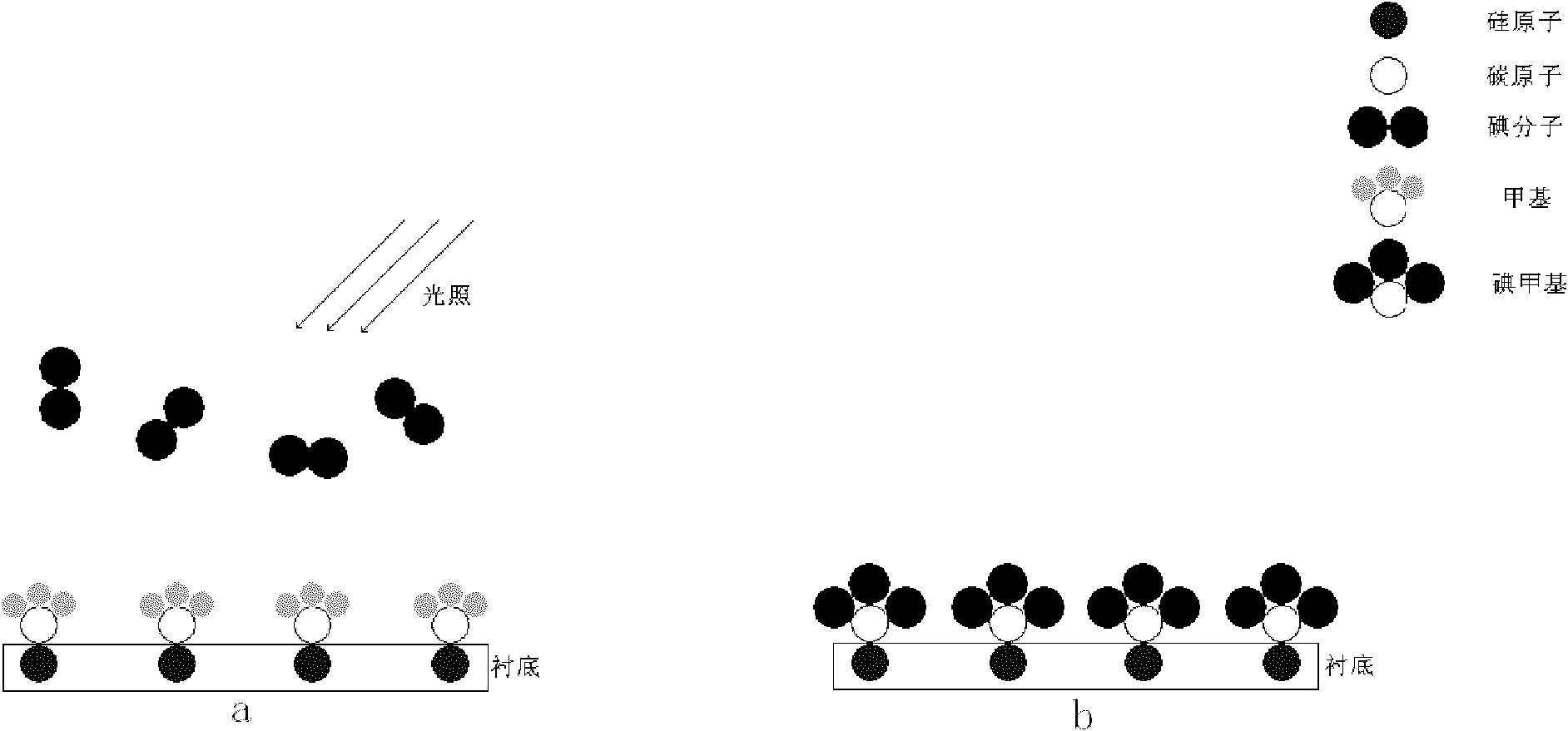
[0032] Step 102, placing the hydrogenated silicon substrate in the reaction chamber of the atomic layer deposition equipment; passing argon gas with a concentration of 99.99% into the reaction chamber of the atomic layer deposition equipment for 5 minutes to clean the reaction chamber; Pass diazomethane into the reaction chamber for 5 minutes, and at the same time irradiate with ultraviolet light with a wavelength of 285nm to decompose diazomethane, and the decomposition products have unbonded electrons. The chemical expression of diazomethane decomposition is: Such as figure 1 As shown in Figure b;
[0033] The decomposition product carbene (: CH2)...
Embodiment 2
[0038] A method for preparing a single crystal cubic carbon nitride film, comprising the steps of:
[0039] Step 101, under 300°C plasma conditions, treat the surface of the silicon (111) substrate with hydrogen gas for 10 minutes, so that Si-H bonds are formed on the surface of the silicon substrate, such as figure 1 As shown in figure a;
[0040] Step 102, placing the hydrogenated silicon substrate in the reaction chamber of the atomic layer deposition equipment; passing argon gas with a concentration of 99.99% into the reaction chamber of the atomic layer deposition equipment for 5 minutes to clean the reaction chamber; Pass diazomethane into the reaction chamber for 10 minutes, and at the same time, irradiate with ultraviolet light with a wavelength of 300nm to decompose diazomethane, and the decomposition products have unbonded electrons. The chemical expression of diazomethane decomposition is: Such as figure 1 As shown in Figure b;
[0041] The decomposition product...
Embodiment 3
[0046] A method for preparing a single crystal cubic carbon nitride film, comprising the steps of:
[0047] Step 101, under 400°C plasma conditions, treat the surface of the silicon (111) substrate with hydrogen gas for 15 minutes, so that Si-H bonds are formed on the surface of the silicon substrate, such as figure 1 As shown in figure a;
[0048] Step 102, placing the hydrogenated silicon substrate in the reaction chamber of the atomic layer deposition equipment; passing argon gas with a concentration of 99.99% into the reaction chamber of the atomic layer deposition equipment for 5 minutes to clean the reaction chamber; Pass diazomethane into the reaction chamber for 15 minutes, and at the same time irradiate with ultraviolet light with a wavelength of 320nm to decompose diazomethane, and the decomposition products have unbonded electrons. The chemical expression of diazomethane decomposition is: Such as figure 1 As shown in Figure b;
[0049] The decomposition product ...
PUM
| Property | Measurement | Unit |
|---|---|---|
| Wavelength | aaaaa | aaaaa |
| Wavelength | aaaaa | aaaaa |
| Wavelength | aaaaa | aaaaa |
Abstract
Description
Claims
Application Information


