Eureka AIR delivers breakthrough ideas for toughest innovation challenges, trusted by R&D personnel around the world.

Method for reducing operation power consumption of phase change memory unit

A phase-change memory, cell operation technology, applied in static memory, digital memory information, information storage, etc., to achieve the effect of reducing operating voltage and operating power consumption

Inactive Publication Date: 2013-08-14
TONGJI UNIV
View PDF5 Cites 0 Cited by
  • Summary
  • Abstract
  • Description
  • Claims
  • Application Information

AI Technical Summary

Problems solved by technology

However, using dielectric materials with a perovskite structure, such as BaTiO 3 , SrTiO 3 The research of etc. has not been reported yet

Method used


Image

  • Method for reducing operation power consumption of phase change memory unit
  • Method for reducing operation power consumption of phase change memory unit
  • Method for reducing operation power consumption of phase change memory unit

Examples


Embodiment 1

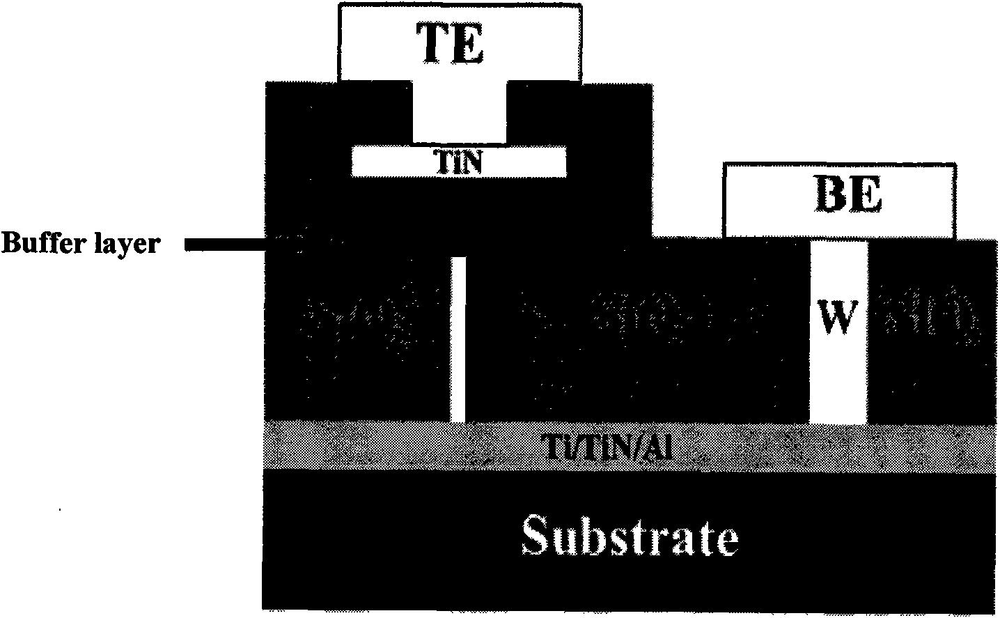
[0022] Adoption of BaTiO in Phase Change Memory Devices 3 as a buffer layer.

[0023] a. SiO after photolithography treatment by magnetron sputtering 2 / Si substrate prepared BaTiO with a thickness of 10nm 3 Thin film, the sputtering power is 20W, oxygen and argon gas are passed through during sputtering, and the ratio of oxygen partial pressure to argon partial pressure is 1:3.

[0024] b. The prepared BaTiO 3 The film was annealed in an oxygen atmosphere for 10 minutes at a temperature of 400° C. to obtain the final buffer layer material.

[0025] c. SiO coated with buffer layer material 2 GST phase-change material with a thickness of 150nm was prepared by magnetron sputtering on the / Si substrate, and packaged into a phase-change memory device.

Embodiment 2

[0027] The use of SrTiO in phase change memory devices 3 as a buffer layer.

[0028] a. SiO after photolithography treatment by magnetron sputtering 2SrTiO with a thickness of 10nm was prepared on a Si substrate 3 Thin film, the sputtering power is 20W, oxygen and argon gas are passed through during sputtering, and the ratio of oxygen partial pressure to argon partial pressure is 1:3.

[0029] b. The prepared SrTiO 3 The film was annealed in an oxygen atmosphere for 10 minutes at a temperature of 400° C. to obtain the final buffer layer material.

[0030] c. SiO coated with buffer layer material 2 GST phase-change material with a thickness of 150nm was prepared by magnetron sputtering on the / Si substrate, and packaged into a phase-change memory device.

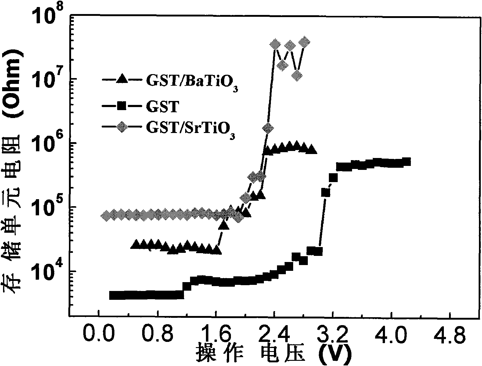
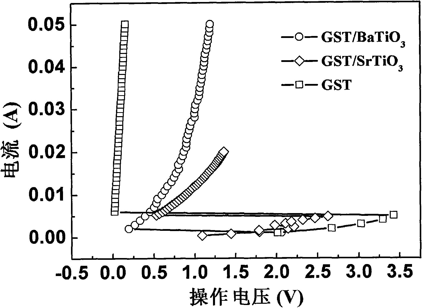
[0031] The test of the resistance-voltage and current-voltage performance during the reset process of the phase change memory device is to use the Agilent-81104A pulse signal generator to output a specific voltage pulse,...


PUM

PropertyMeasurementUnit
Thicknessaaaaaaaaaa
Thicknessaaaaaaaaaa

Abstract

The invention relates to a method for reducing unit operation power consumption of a phase change memory, comprising the following steps of: (1) coating a BaTiO3 or SrTiO3 dielectric thin film on a SiO2 / Si substrate; (2) annealing the SiO2 / Si substrate coated with the dielectric thin film in the step (1) to obtain a SiO2 / Si substrate with a buffer layer; and (3) coating GST phase change material on the SiO2 / Si substrate which is provided with the buffer layer and prepared in step (2)and packaging into a phase change memory device. In the invention, the dielectric substance with a perovskite structure serves as the buffer layer and the unit operation voltage of the phase change memory can be effectively reduced, and therefore, the power consumption can be reduced.

Description

technical field [0001] The invention belongs to the field of electronic functional materials and devices, and in particular relates to a method for reducing the operating power consumption of a phase-change memory unit by using a dielectric as a buffer layer. The method fully meets the technical requirements of silicon integration technology. Background technique [0002] Phase change memory (PCM) mainly uses certain materials to have a fast and reversible phase change effect under a specific current pulse, which leads to a stable change in certain characteristics of the material to achieve the storage effect. In addition, its final state It will not change with the disappearance of the external energy, so it has the characteristics of non-volatility. With its advantages in read speed, reliability, non-destructive read, non-volatility, miniaturized size and cost, PCM technology has been recognized as the most potential to replace traditional DRAM technology and Flash memory ...

Claims


Application Information

Patent Timeline
IPC IPC(8): H01L45/00G11C11/56
Inventor 翟继卫尚飞
Owner TONGJI UNIV
Why Eureka
Eureka Blog
Learn More