Composite material stripline waveguide array antenna

A technology of composite materials and waveguide arrays, which is applied to antenna arrays, antennas, antenna supports/mounting devices, etc., can solve the problems of relatively stringent weight requirements for microwave antennas, reduce material costs, overcome complex structures, and have good sealing performance Effect

Inactive Publication Date: 2011-07-06
中国兵器工业第二0六研究所
3 Cites 9 Cited by

AI-Extracted Technical Summary

Problems solved by technology

[0004] The technical problem to be solved by the present invention: Aiming at the shortcomings of the traditional stripline in terms of electrical performance and structure, a composite stripline waveguide and a composite stripline waveguide radiation unit are used as the basis The linear waveguide array antenna solves the problem that the weight requirements of microwave antennas in radar or communication systems are relatively ha...

Abstract

The invention discloses a composite material stripline waveguide array antenna, which is designed on the basis of a novel composite material stripline waveguide and a composite material stripline waveguide radiation unit, and is mainly used in microwave antennas in the field of radar and communication. The composite material stripline waveguide array antenna is made of 13 layers of flat materials, such as an array antenna inner conductor, a feed power divider single-sided copper clad layer, an array antenna outer conductor, a radiation slot speaker array single-sided copper clad layer, a stripline inner film layer, a medium support layer, a reinforcement layer, a stripline outer film layer and the like, with different thicknesses, by high-temperature machining processes of a bag pressing or die pressing method. The composite material stripline waveguide array antenna has the characteristics of low loss, light weight, stable structure, simple machining, low cost, high sealing performance and the like. The machined linear array antenna has the external dimension of 2,400mm*200mm*10.8mm and the weight of only 1.2 kg.

Application Domain

Antenna arraysAntenna supports/mountings

Technology Topic

PhysicsLinear array +9

Image

  • Composite material stripline waveguide array antenna
  • Composite material stripline waveguide array antenna
  • Composite material stripline waveguide array antenna

Examples

  • Experimental program(1)

Example Embodiment

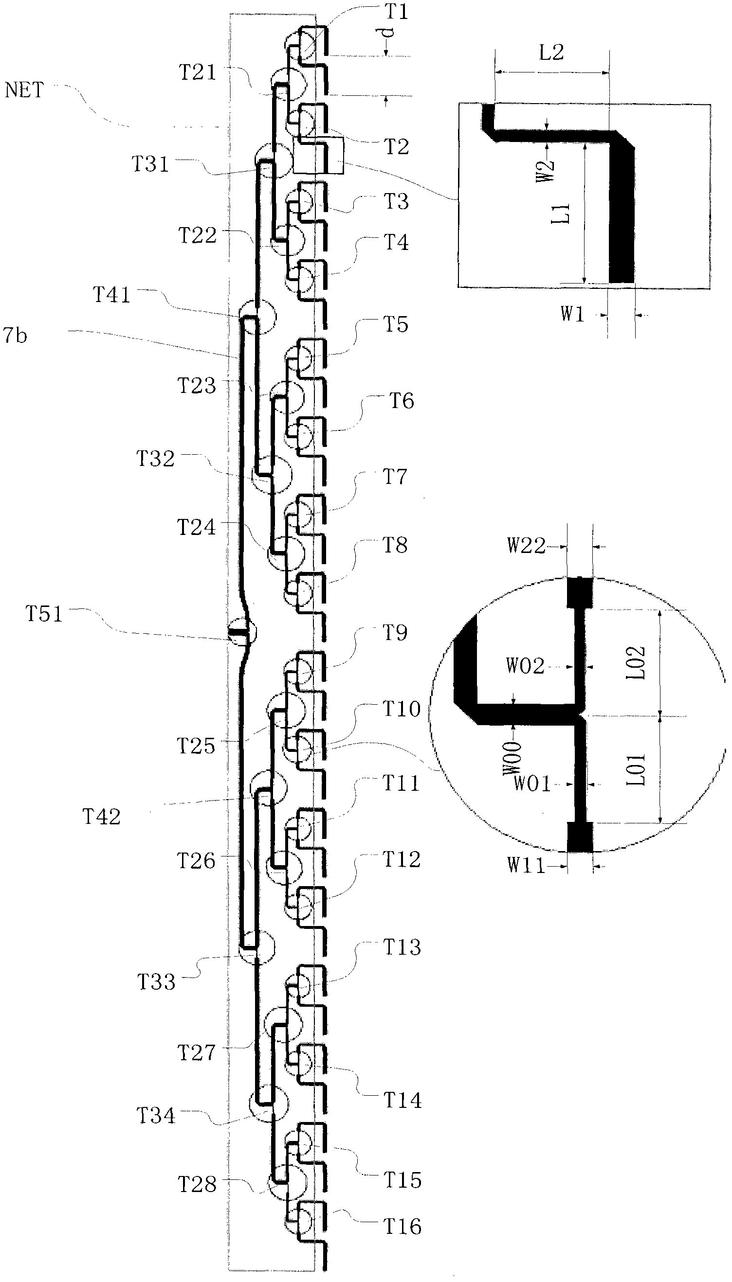
[0014] The design frequency band of the present invention is S-band 3.1GHz~3.4GHz, the number of array units is 32, and the unit spacing d=72mm. With reference to the above drawings, the present invention will be further explained through embodiments.
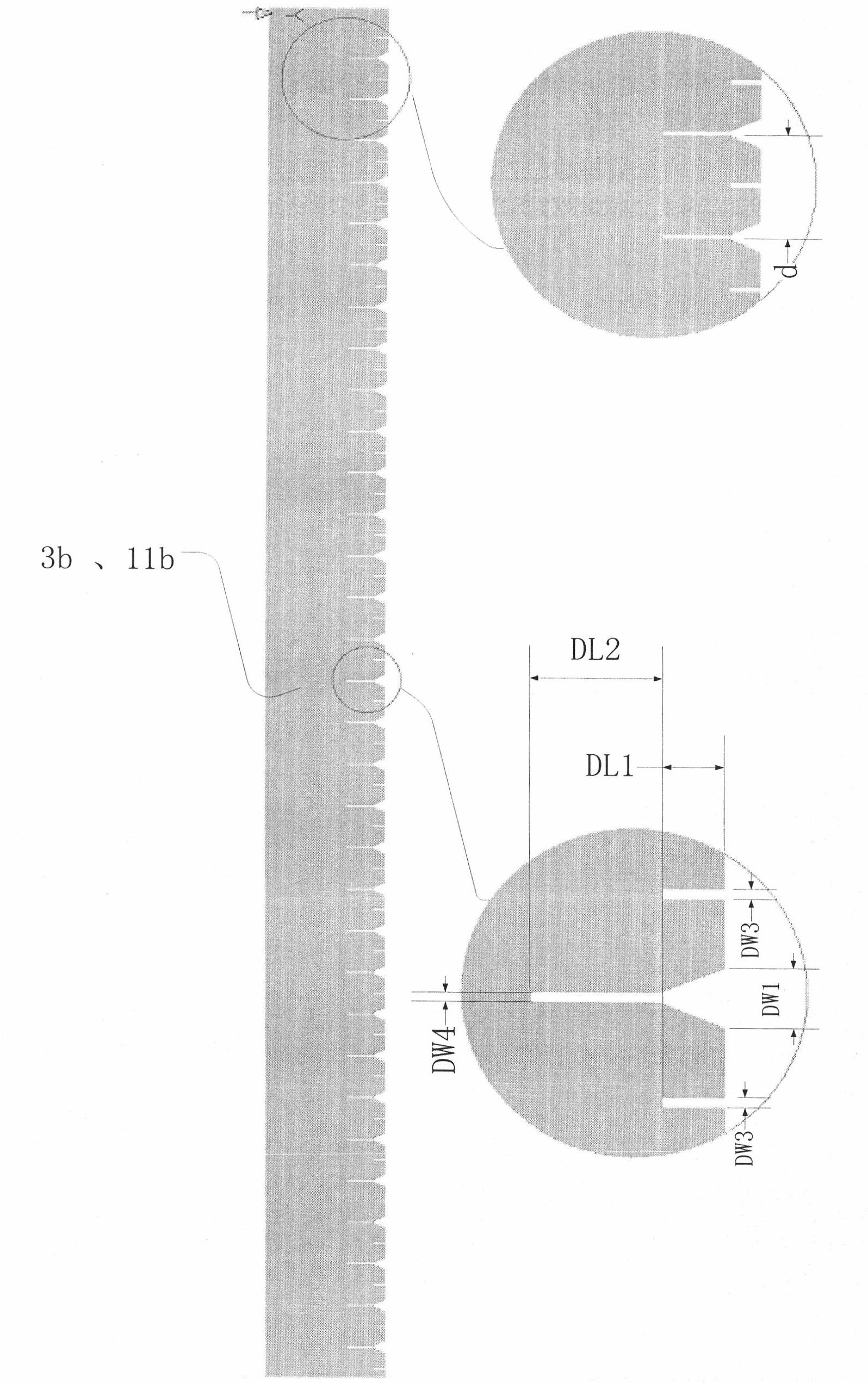
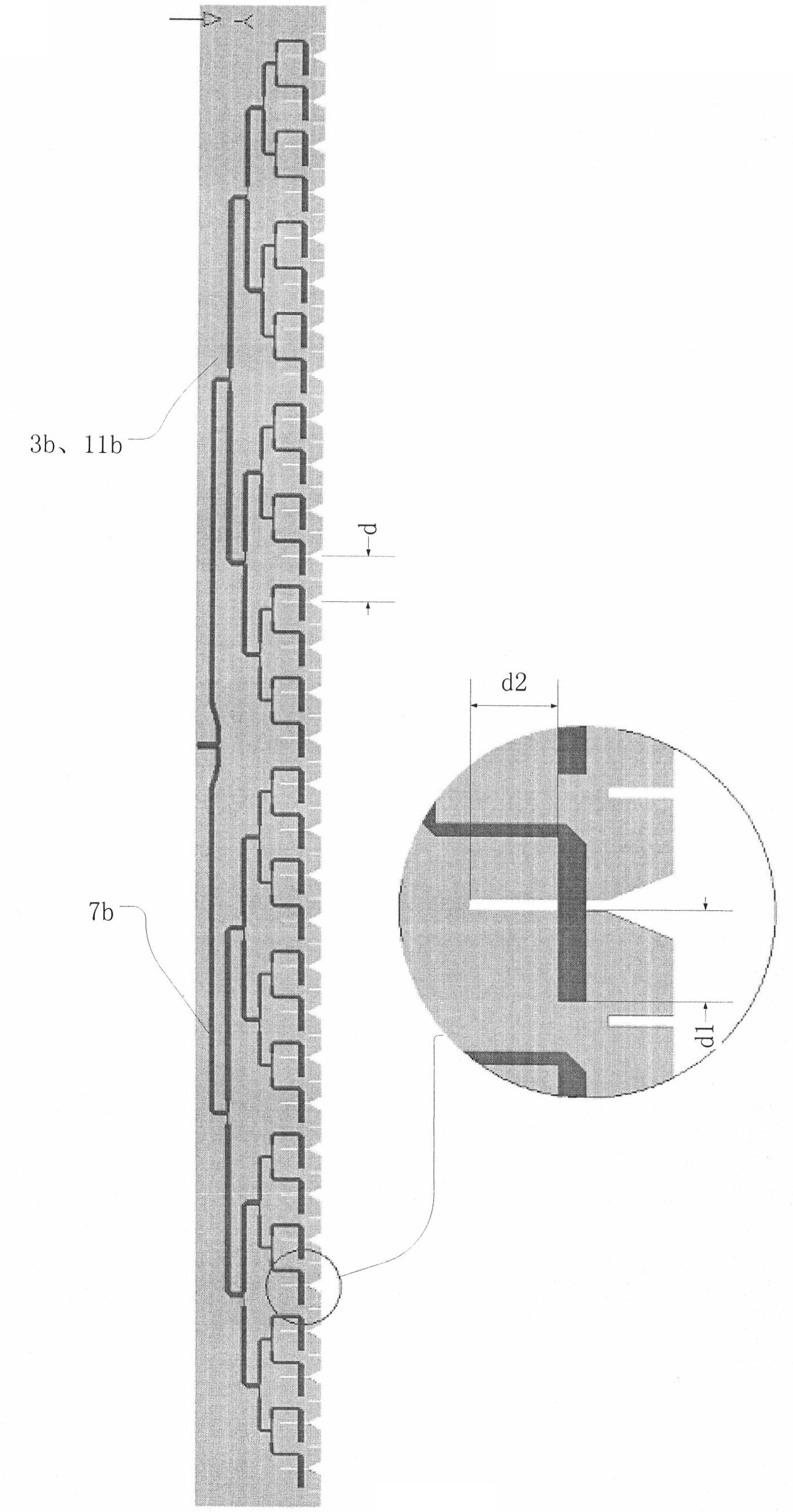
[0015] Such as figure 2 As shown, two LPI halogen-free polyimide film single-sided copper-clad laminates 3 and 11 are used, one front and the other are used as the outer conductor of the composite stripline array antenna, and the front and the other are printed at the same time. Two equally spaced radiating slot horns and isolation slots such as figure 2 The 3b and 11b shown as the radiating slot horn array of the array antenna. Such as figure 1 As shown, another piece of LPI halogen-free polyimide film single-sided copper-clad laminate is used as the center conductor of the composite strip line array antenna, on which the inner conductor and the strip line power points divided into 32 are printed The open circuit of the feeder and 32 radiating elements is used as the feeder power divider of the composite stripline array antenna.
[0016] Such as figure 1 The feed network NET printed on the center conductor of the composite stripline array antenna includes a five-layer one-to-two power splitter (T1~T16, T21~T28, T31~T34, T41~ T42, T51), the input of each layer of feed power divider is connected to the branch output of one layer of feed power divider. The size of each feed power divider is composed of the combined port line width W00 and the two branch port line width W11 , W22, the corresponding conversion section line width W01, W02, the length of the conversion section L01, L02 and other parameters are uniquely determined, the size of each feeder power divider is not the same; the width of each feed opening line W1, length L1, the width W2 and the length L2 of the feeder connected to it, all the feeder opening routes are the same; the distance between adjacent feeder opening routes is d=72mm. figure 1 See Table 1 for the size of each feeder power divider in.
[0017] Such as figure 2 As shown, there is an isolation slot between each adjacent radiating slot horn on the outer conductor of the composite strip line array antenna, and the equal distance between the radiating slot horn and the isolation slot is d=72mm. The figure size of the radiating slot horn and the isolation slot is listed in Table 2.
[0018] Such as Figure 4 As shown, the names and thicknesses of the 13-layer flat materials of the present invention are:
[0019] The first layer of flame-retardant epoxy woven fabric prepreg, 0.2mm thick, and its curing temperature is about 130 degrees Celsius;
[0020] The second layer of epoxy film, 0.1mm thick, its curing temperature is about 130 degrees Celsius;
[0021] The outer conductor and radiating slot horn array on the third layer array antenna are made of LPI halogen-free polyimide film copper clad laminate, 0.035mm thick, printed on it figure 2 The figure shown, the figure size is shown in Table 2;
[0022] The fourth layer of AFA halogen-free acrylic film, 0.05mm thick, its curing temperature is about 160 degrees Celsius;
[0023] The fifth layer of PMI polymethacrylimide foam, 5mm thick;
[0024] The sixth layer of AFA halogen-free acrylic film, 0.05mm thick, its curing temperature is about 160 degrees Celsius;
[0025] The 7th layer of array antenna inner conductor and feed power divider, made of LPI halogen-free polyimide film copper clad laminate, 0.035mm thick, printed on it figure 1 The figure shown, the figure size is shown in Table 1;
[0026] The eighth layer of AFA halogen-free acrylic film, 0.05mm thick, its curing temperature is about 160 degrees Celsius;
[0027] The 9th layer of PMI polymethacrylimide foam, 5mm thick;
[0028] The tenth layer of AFA halogen-free acrylic film, 0.05mm thick, its curing temperature is about 160 degrees Celsius;
[0029] The lower outer conductor of the 11th layer array antenna and the radiating slot horn array, made of LPI halogen-free polyimide film copper clad laminate, 0.035mm thick, printed on it figure 2 The figure shown, the figure size is shown in Table 2;
[0030] The 12th layer of epoxy film, 0.1mm thick, its curing temperature is about 130 degrees Celsius;
[0031] The 13th layer of flame-retardant epoxy woven fabric prepreg, 0.2mm thick, and its curing temperature is about 130 degrees Celsius;
[0032] First, follow the 3rd to 11th floors Figure 4 Stacked in the order and direction shown, the relative position dimensions between the 3, 7, and 11 layers are shown in Table 4. After the bag pressing method is used for high temperature bonding at about 160 degrees Celsius, follow the figure 1 Stack 1, 2 and 12, 13 layers in the order and direction shown, and glue them together at a high temperature of about 130 degrees Celsius by bag pressing to make Figure 5 The composite stripline waveguide array antenna shown. The thickness of the finished stripline waveguide is 10.8mm±0.1mm, the length is 2400mm, the width is 200mm, and its weight is 1200g. See the test pattern Image 6. The sidelobe level is below -30dB in the entire frequency band.
[0033] Table 1 Size table of 31 (T1~T31) 1 point 2 feed power dividers
[0034] Serial number
[0035] T7
[0036] T51
[0037] Table 2 Slot speaker size table
[0038] DW1(mm)
[0039] Table 3 Size table of feed opener
[0040] W1(mm)
[0041] Table 4 Dimensions of the relative position of the slot horn and the feed opener
[0042] D1(mm)

PUM

PropertyMeasurementUnit
Thickness0.035mm
Thickness0.05mm
Thickness5.0mm

Description & Claims & Application Information

We can also present the details of the Description, Claims and Application information to help users get a comprehensive understanding of the technical details of the patent, such as background art, summary of invention, brief description of drawings, description of embodiments, and other original content. On the other hand, users can also determine the specific scope of protection of the technology through the list of claims; as well as understand the changes in the life cycle of the technology with the presentation of the patent timeline. Login to view more.

Similar technology patents

Electric blower and electric vacuum cleaner utilizing the same

InactiveUS20110277267A1high suction performancereduce loss
Owner:PANASONIC CORP

Motor system

InactiveUS20120194108A1reduction in switch frequencyreduce loss
Owner:HONDA MOTOR CO LTD

Intelligent drying control method for washing machine

ActiveCN103334255Areduce running timereduce loss
Owner:PANASONIC APPLIANCES CHINA CO LTD +1

Non-annealed cold forging steel hot-rolled wire rod and production method thereof

InactiveCN104988409AReduce work hardeningreduce loss
Owner:XINGTAI IRON & STEEL

Classification and recommendation of technical efficacy words

  • stable structure
  • reduce loss

Silicon/carbon composite microsphere negative electrode material as well as preparation method and application for same

ActiveCN103311522Astable structureImprove charge and discharge cycle life
Owner:INST OF PROCESS ENG CHINESE ACAD OF SCI

Preparation method of magnetic graphene based oil absorption foam material

Owner:XINJIANG TECHN INST OF PHYSICS & CHEM CHINESE ACAD OF SCI
Why Eureka
Try Eureka