Memory based on self-assembled QD (Quantum Dots) and preparation method thereof

A technology of self-organized quantum dots and memory, which is applied in semiconductor/solid-state device manufacturing, semiconductor devices, electrical components, etc., can solve the problems of long writing time and short life, and achieve improved device life, fast speed, and mature methods Effect

Inactive Publication Date: 2013-01-02
INST OF SEMICONDUCTORS - CHINESE ACAD OF SCI
View PDF0 Cites 0 Cited by
  • Summary
  • Abstract
  • Description
  • Claims
  • Application Information

AI Technical Summary

Problems solved by technology

The two layers of SiO 2 While the potential barrier realizes non-volatile storage, it also causes two major shortcomings of Flash
One is that the write time is longer (~ms), and the other is that the lifespan is short (~10 6 write / erase cycles)

Method used


Image

  • Memory based on self-assembled QD (Quantum Dots) and preparation method thereof
  • Memory based on self-assembled QD (Quantum Dots) and preparation method thereof
  • Memory based on self-assembled QD (Quantum Dots) and preparation method thereof

Examples


Embodiment Construction

[0038] In order to make the object, technical solution and advantages of the present invention clearer, the present invention will be described in further detail below in conjunction with specific embodiments and with reference to the accompanying drawings.

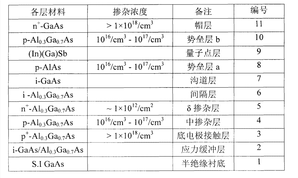
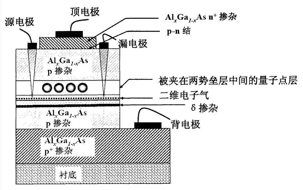
[0039] The device material of the present invention is grown on solid source molecular beam epitaxy (MBE) equipment, and can also be grown by metal oxide chemical vapor deposition (MOCVD). exist figure 1 The device structure fabricated on the material structure shown is as follows figure 2 :

[0040] 1. The (100) GaAs semi-insulating substrate 1 is used to reduce substrate leakage current.

[0041] 2. Growth stress buffer layer 2 on GaAs semi-insulating substrate 1: This layer is an undoped semiconductor material, the purpose is to obtain a high-quality epitaxial layer and reduce the influence of defects in the substrate on the electronic channel layer , the thickness needs above. A thicker stress buffer layer will...


PUM


Abstract

The invention discloses a memory based on self-assembled QD (Quantum Dots) and a preparation method thereof. The memory utilizes QDs as a carrier storage unit and presents the two states (zero or one) of an information bit by two charging states of the QDs which are arranged in a p-n junction depletion area and realize the write-in and storage operations of the memory by utilizing the depletion area. A 2DEG (Two-Dimensional Electronic Gas) trench layer is arranged below the QD layer and beyond the p-n junction depletion area and realizes the read-out and erasing operations of the memory thereby. The invention has a simple structure and a simple and effective preparation process, combines the advantages of mainstream memories of DRAMs (Dynamic Random Access Memories) and flash memories on current markets, has the advantages of high speeds in reading, writing and erasing, nonvolatile memory, long service life, less electricity consumption, low working voltage, and the like and is also afeasible method for realizing high-speed logic.

Description

technical field [0001] The invention relates to the field of semiconductor materials and devices, in particular to a memory based on self-organized quantum dots and a preparation method thereof. Background technique [0002] In today's semiconductor memory market, there are two important products: dynamic random access memory (DRAM) and flash memory (Flash Memory). Among them, DRAM has the advantages of fast reading, writing and erasing speed (~20nm) and long life (~10nm). 15 write / erase cycles) have long been the most common memory in computers, exchanging data directly with the central processing unit (CPU). But DRAM can only keep data for a short time (~ms), that is, it is volatile, and it must be refreshed once in a while in order to keep the data. If the storage unit is not refreshed, such as power off, The stored information will be lost. At the same time, DRAM consumes a lot of power. These two disadvantages make it unsuitable for mobile applications. [0003] A...

Claims


Application Information

Patent Timeline
Patent Type & Authority Patents(China)
IPC IPC(8): H01L29/772H01L29/778H01L21/335
Inventor 李越强王晓东徐晓娜刘雯陈燕玲杨富华
Owner INST OF SEMICONDUCTORS - CHINESE ACAD OF SCI
Why Eureka
Try Eureka