Preparation method of field blocking type bipolar transistor of insulated gate

A bipolar transistor, insulated gate technology, applied in semiconductor devices, semiconductor/solid-state device manufacturing, electrical components, etc., can solve the problems of complex sheet process operations, high fragmentation rate, and high process costs.

Active Publication Date: 2011-08-03
MACMIC SCIENCE & TECHNOLOGY CO LTD
View PDF3 Cites 31 Cited by
  • Summary
  • Abstract
  • Description
  • Claims
  • Application Information

AI Technical Summary

Problems solved by technology

Because the backside process of the silicon wafer has come to the end of the process, and the device structure on the front side of the silicon wafer has been formed, high-temperature thermal diffusion cannot be carried out later, and the field blocking layer needs a certain depth, so only laser annealing can be used, but the backside process requires Both the ultra-high-energy ion implanter and the laser annealing furnace are very expensive, and the operation of the thin slice process is also very complicated, with a high fragmentation rate, resulting in high overall process costs

Method used


Image

  • Preparation method of field blocking type bipolar transistor of insulated gate
  • Preparation method of field blocking type bipolar transistor of insulated gate
  • Preparation method of field blocking type bipolar transistor of insulated gate

Examples


Embodiment Construction

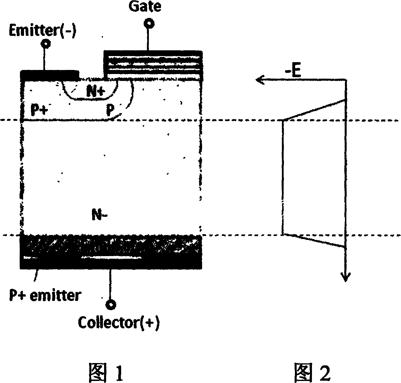
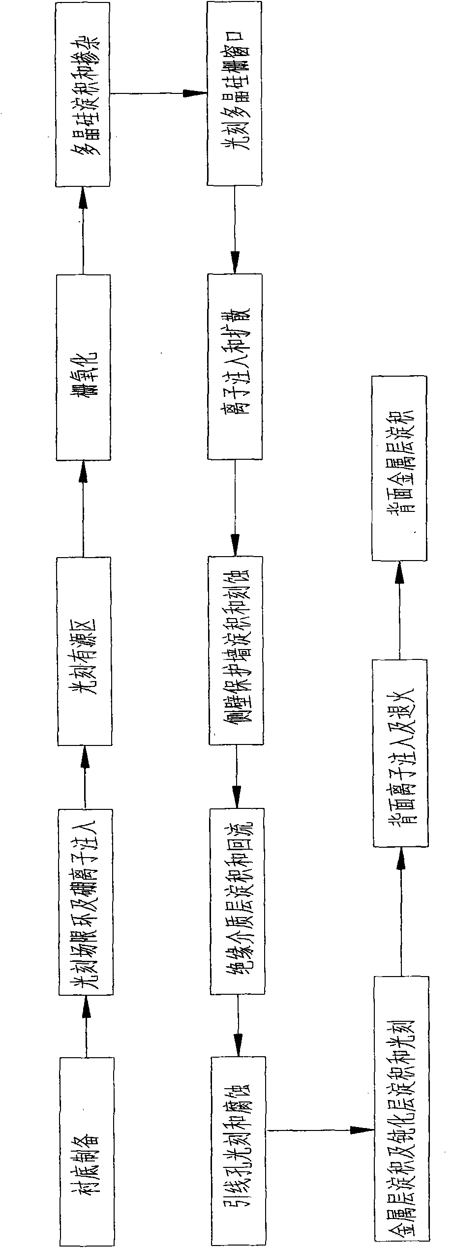
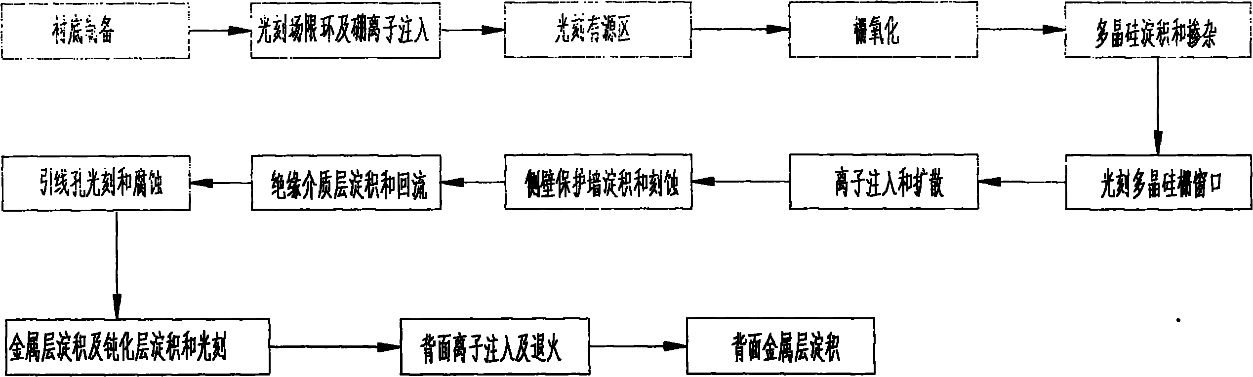
[0023] See image 3 As shown, the method for preparing a field-stop type insulated gate bipolar transistor of the present invention comprises the following steps:

[0024] (1) Substrate preparation: After cleaning the N-type single wafer with a thickness of 100-1000 μm, the resistivity of the N-type single wafer is 10-300Ω·cm, Pre-diffusion of N+-type semiconductor impurities on the surface with a concentration higher than that of N- single wafers can be pre-diffused with a phosphorus source, and then at a temperature of 1100-1300°C, the main diffusion of N+-type impurities is performed for 100-400h, and the junction depth is pushed to 10-300μm Form the N+ impurity region. In the main diffusion of the N+ type impurity in the present invention, the N+ type impurity diffusion can be carried out at a temperature of 1150-1250°C for 150-200h, and the junction depth can be pushed to 50-200μm to form the N+ impurity region. The formed oxide layers on both sides can prevent a large a...


PUM


Abstract

The invention relates to a preparation method of a field blocking type bipolar transistor of an insulated gate, which comprises the following steps of: pre-diffusing N+ type semiconductor impurities on a positive surface and a negative surface of an N-type single wafer after the N-type single wafer is cleaned; forming N+ impurity regions through main diffusion and knotting; removing one N+ impurity region as a front surface of a silicon wafer through grinding; polishing the front surface of the silicon wafer to obtain a substrate material; photoetching a field-limiting ring to form a P+ window of the field-limiting ring; performing boron ion injection; forming a window of a source region through photoetching; performing polysilicon deposition and doping after a silicon wafer gate is oxidized; injecting ions in the window of the silicon wafer gate, and forming a P impurity region and an N+ impurity region through diffusion; depositing and refluxing an insulated dielectric layer, photoetching a lead hole and depositing a metal layer to form an emitting electrode and a grid electrode; thinning the N+ impurity region at the back of the silicon wafer through grinding; annealing the N+ impurity region to form a P+ impurity region after the boron ions are injected in the N+ impurity region; and depositing a metal layer to form a collecting electrode. The method has the characteristics of having simplified process flow, achieving low production cost, and being beneficial for realizing the soft turn-off of an IGBT (Insulated Gate Bipolar Translator).

Description

technical field [0001] The invention relates to a method for preparing a field-blocking insulated gate bipolar transistor, which belongs to the technical field of semiconductor devices. Background technique [0002] Due to the increasing proportion of insulated gate bipolar transistors (IGBTs) used in consumer electronics products such as induction cookers, frequency conversion appliances, and digital cameras, and the huge impact of the overall output of consumer electronics products, IGBTs have become a new force in the family of power devices. Field-blocking insulated-gate bipolar transistors (FS-IGBTs) have continuously expanded their application range due to a series of excellent properties such as low switching loss and on-state voltage drop compatibility, high short-circuit capability, and easy parallel connection. See figure 1 , 2 As shown, for the field-blocking insulated gate bipolar transistor, since the N+stop layer is the field-stopping layer, its concentration...

Claims


Application Information

Patent Timeline
Patent Type & Authority Applications(China)
IPC IPC(8): H01L21/331H01L21/28H01L21/223H01L21/265
Inventor 戚丽娜张景超刘利峰赵善麒
Owner MACMIC SCIENCE & TECHNOLOGY CO LTD
Why Eureka
Try Eureka