Method for building silicon-based coupling resonance loop structure capable of providing stimulated Raman scattering light grain

A technology of stimulated Raman scattering and coupled resonance, applied in the directions of light guides, optics, optical components, etc., can solve the problems of no advantage, propagation light loss, etc., to achieve high sensitivity, compensation loss, and enhanced signal-to-noise ratio.

Active Publication Date: 2011-08-10
BEIHANG UNIV
View PDF3 Cites 8 Cited by
  • Summary
  • Abstract
  • Description
  • Claims
  • Application Information

AI Technical Summary

Problems solved by technology

However, in the process of scientific experiments and engineering implementation, due to the material properties (such as light absorption and scattering, etc.) and structural characteristics (such as bending radius light loss, etc.) Seriously affect the performance of the coupling resonator ring as the core component of the optical waveguide gyroscope, so that the existence of optical loss makes the optical waveguide gyroscope have no advantage compared with the traditional fiber optic gyroscope under the condition of given loss and size

Method used


Image

  • Method for building silicon-based coupling resonance loop structure capable of providing stimulated Raman scattering light grain
  • Method for building silicon-based coupling resonance loop structure capable of providing stimulated Raman scattering light grain
  • Method for building silicon-based coupling resonance loop structure capable of providing stimulated Raman scattering light grain

Examples


Embodiment

[0018] Embodiment: Below in conjunction with accompanying drawing, the present invention will be further described. See Figure 4 , the present invention is a method for constructing a silicon-based coupled resonant ring structure that provides stimulated Raman scattering light gain. The specific steps of the method are as follows:

[0019] Step 1. Use ion implantation and other methods to implant oxygen ions under the surface of pure single crystal silicon by controlling the energy of the ion beam, thereby forming a layer of SiO with a thickness of 1 μm at 1.55 μm below the surface. 2 Buried layer, thus making the SOI substrate.

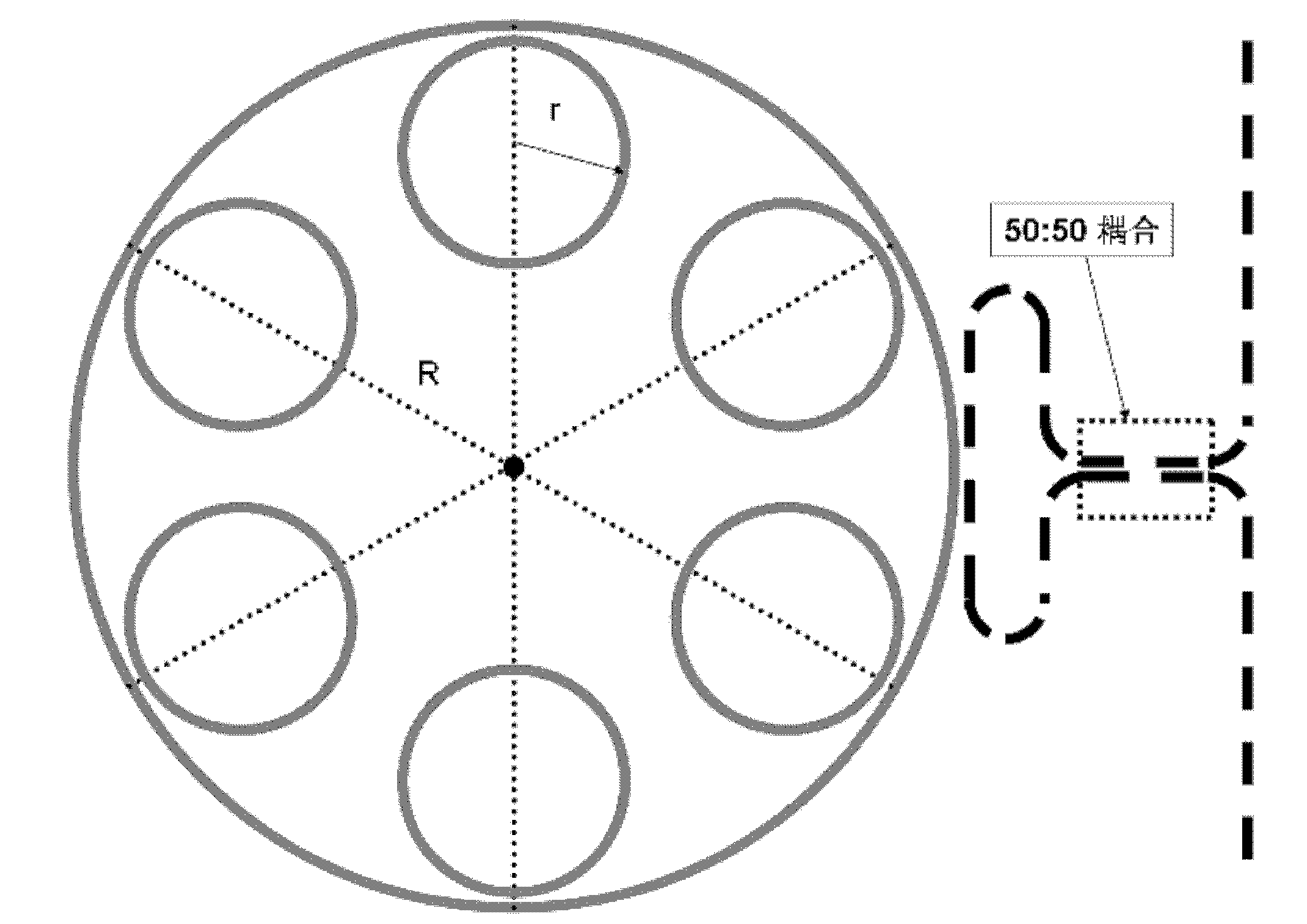
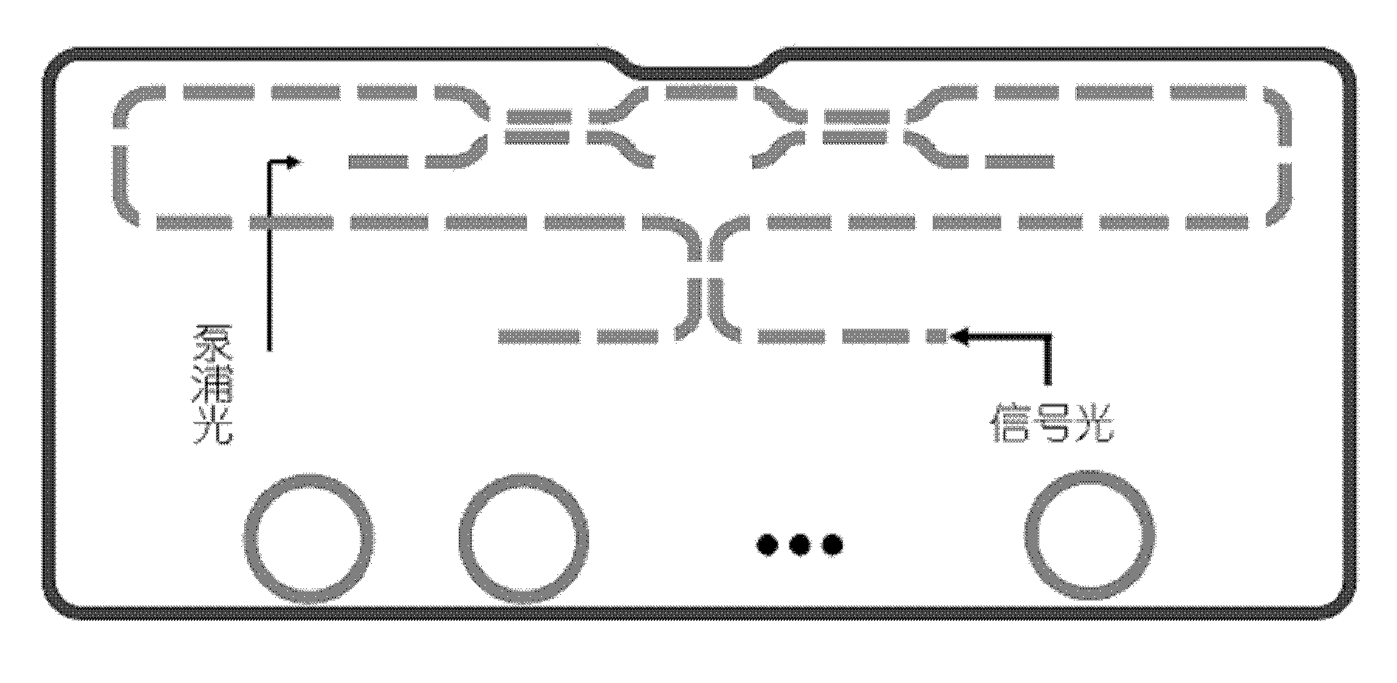
[0020] Step 2. Since in the actual microelectronic etching process, figure 1 The large circular ring waveguide shown is too difficult to realize, so it is designed as image 3 Equivalent optical path shown. That is to replace the peripheral circular closed-loop waveguide with a rectangular closed-loop waveguide, and the small-sized ring waveguid...


PUM


Abstract

The invention relates to a method for building a silicon-based coupling resonance loop structure capable of providing stimulated Raman scattering light grain. The method comprises the following four steps of: 1, making a required silicon on insulator (SOI) substrate on the surface of common pure single-crystal silicon by an ion implantation method; 2, building the silicon-based coupling resonanceloop geometrical light path structure capable of providing the stimulated Raman scattering optical grain on the SOI substrate; 3, building a silicon-based SOI ridge waveguide on the geometrical lightpath structure; and 4, respectively arranging a p+ doped area and an n+ doped area at the left side and the right side of the silicon-base ridge waveguide to form pn junction, and continuously performing a simulated Raman process to generate light grain. By Raman light grain, the loss of transmission light in the structure can be effectively compensated, and the signal-to-noise ratio of the Ramanoptical grain serving as an optical waveguide gyro can be improved. Therefore, by the method, an integrated optical waveguide gyro with high sensitivity can be obtained. Moreover, the method has better practical values and wide application prospects in the technical field of integration of an optical gyro coupling resonance loop.

Description

(1) Technical field [0001] The present invention relates to a coupling resonant ring structure that can provide stimulated Raman scattering light gain and realize the compensation for light loss, and the application of this structure in integrated optical gyroscope, especially relates to a method that provides stimulated Raman scattering. The invention relates to a method for constructing a silicon-based coupled resonant ring structure for scattered light gain, belonging to the technical field of integrated optical gyroscope coupled resonant rings. (2) Background technology [0002] In recent years, a series of breakthroughs in the field of silicon-based photonics integration technology, such as silicon-based Raman lasers, silicon-based high-speed optical modulators, silicon-based photodetectors, etc., have greatly promoted the gradual development of silicon-based photonics into practical fields. . People no longer doubt the possibility that silicon (especially silicon on i...

Claims


Application Information

Patent Timeline
Patent Type & Authority Applications(China)
IPC IPC(8): G02B6/13G02B6/122
Inventor 肖志松燕路邓思盛
Owner BEIHANG UNIV
Why Eureka
Try Eureka