

Method of manufacturing semiconductor element metal gate stack
A metal gate and manufacturing method technology, applied in semiconductor/solid-state device manufacturing, semiconductor devices, electrical components, etc., can solve the problems of component performance change, p-type metal gate resistance increase, etc., to reduce mismatch and RC Delayed, negativity-increased effects
- Summary
- Abstract
- Description
- Claims
- Application Information
AI Technical Summary
Problems solved by technology
Method used
Image

Examples
Embodiment Construction
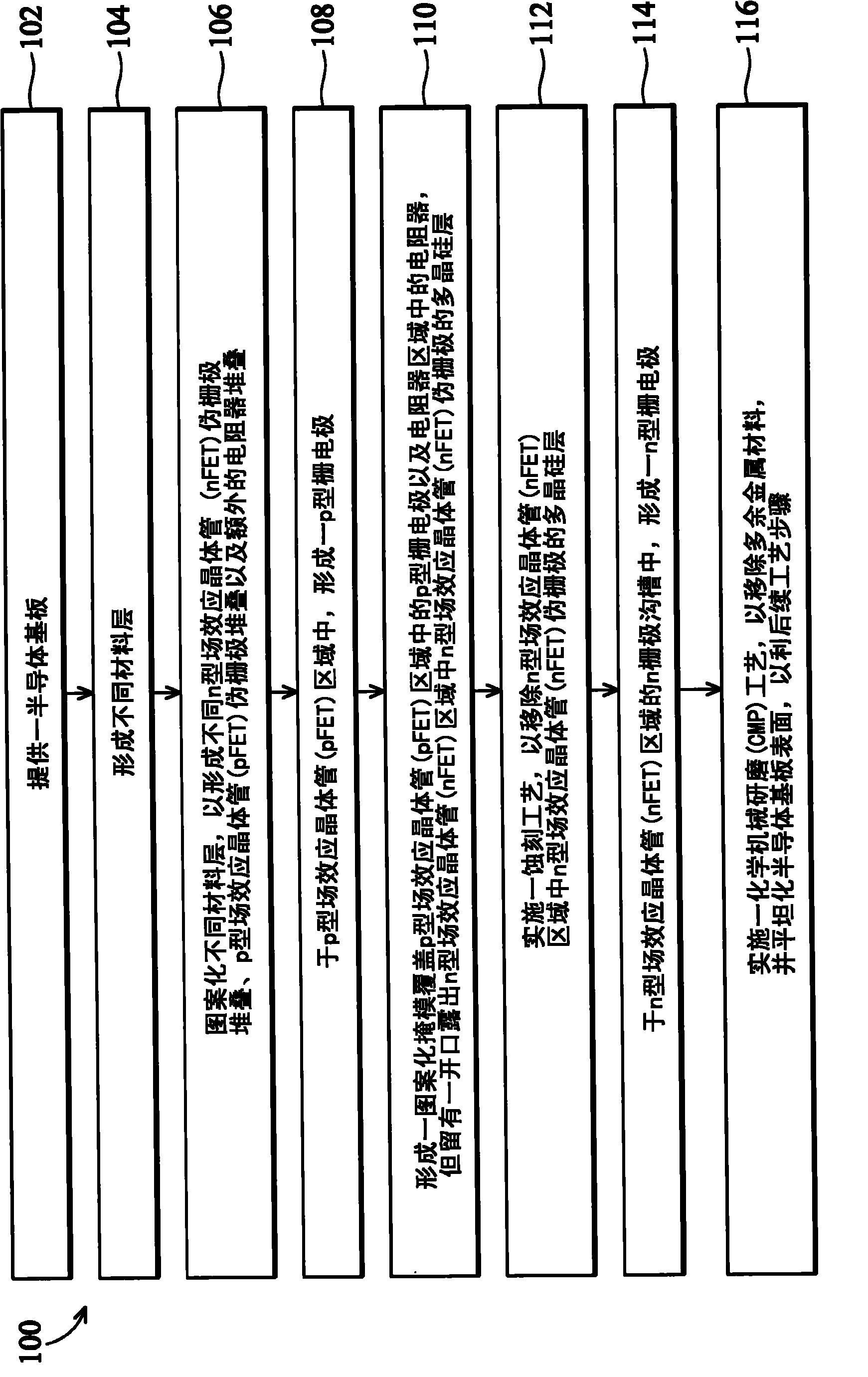
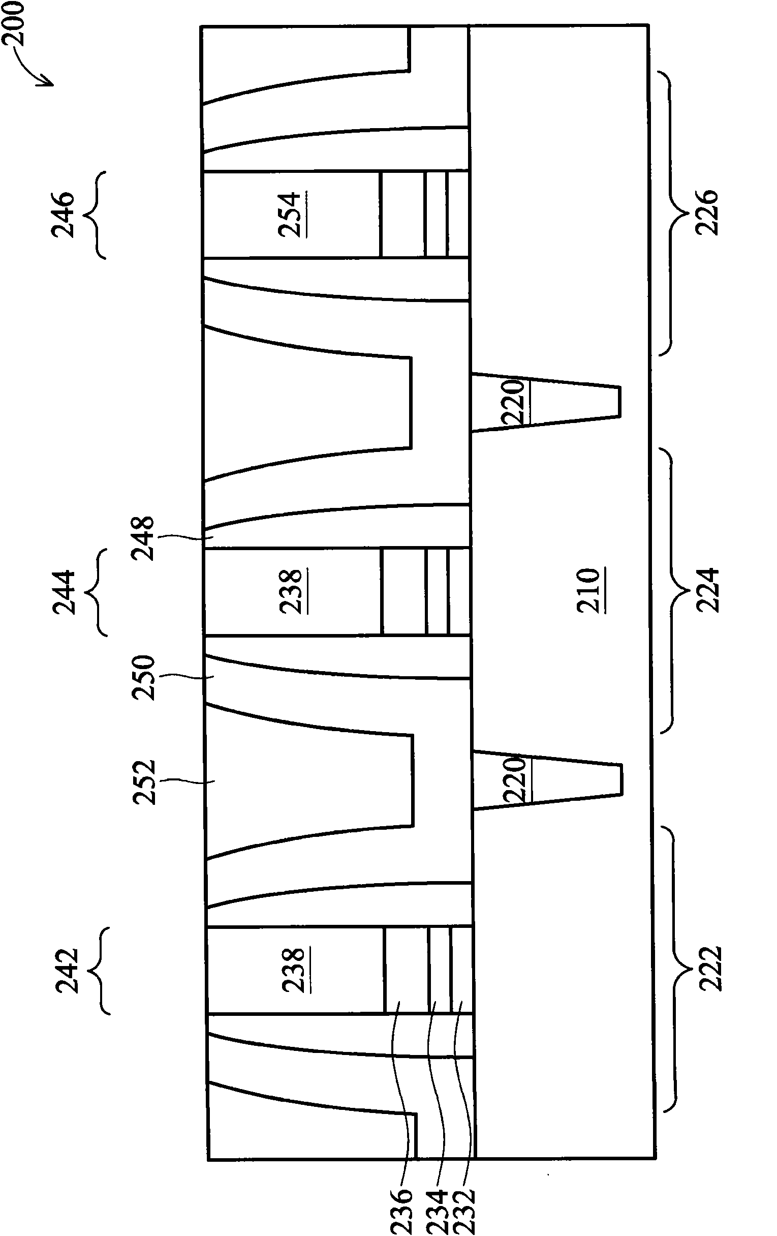
[0039] figure 1 A flowchart of an embodiment of a method 100 for fabricating a semiconductor device having a metal gate stack is disclosed in accordance with various aspects of the present invention. Figure 2 to Figure 7 In view of one or more embodiments of the present invention, schematic cross-sectional views of a semiconductor structure 200 at different process stages are disclosed. For a description of the semiconductor structure 200 and its manufacturing method 100, please refer to Figure 1 to Figure 7 .
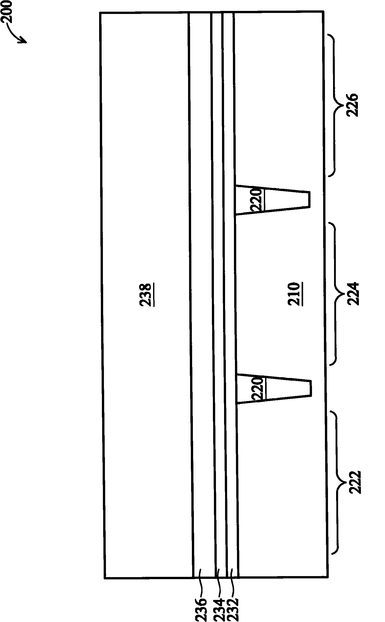
[0040] see figure 1 , figure 2 The method 100 for manufacturing a semiconductor device of the present invention begins at step 102 , providing a semiconductor substrate 210 . The semiconductor substrate 210 includes silicon, and may optionally include germanium, silicon germanium or other suitable semiconductor materials. The semiconductor substrate 210 also includes various isolation structures 220 such as shallow trench isolations formed in the substrate to s...
PUM
| Property | Measurement | Unit |
|---|---|---|
| Thickness | aaaaa | aaaaa |
Abstract
Description
Claims
Application Information