Longitudinal channel SOI (silicon on insulator) nLDMOS (n-type laterally diffused metal oxide semiconductor) device unit with p buried layer

A channel and device technology, applied in the direction of semiconductor devices, electrical components, circuits, etc., can solve the problem of thermal stability affecting the heat dissipation and electrical characteristics of the device, adverse device and system reliability and stability, affecting the withstand voltage performance of the device, etc. to reduce the self-heating effect, improve thermal stability, and improve heat dissipation performance

Active Publication Date: 2011-08-17
SERVICE CENT OF COMMLIZATION OF RES FINDINGS HAIAN COUNTY
View PDF2 Cites 2 Cited by
  • Summary
  • Abstract
  • Description
  • Claims
  • Application Information

AI Technical Summary

Problems solved by technology

In this integrated vertical channel (VC) SOI nLDMOS device, due to the presence of a thick buried oxide layer, the substrate hardly participates in the withstand voltage; when the device encounters a voltage spike during operation, the device is prone to preferential lateral breakdown, which seriously affects the device The improvement of the withstand voltage performance, at the same time, the thicker buried oxide layer will bring serious self-heating effect, which will affect the heat dissipation of the device and the thermal stability of the electrical characteristics, which is not conducive to improving the reliability and stability of the device and system

Method used


Image

  • Longitudinal channel SOI (silicon on insulator) nLDMOS (n-type laterally diffused metal oxide semiconductor) device unit with p buried layer
  • Longitudinal channel SOI (silicon on insulator) nLDMOS (n-type laterally diffused metal oxide semiconductor) device unit with p buried layer
  • Longitudinal channel SOI (silicon on insulator) nLDMOS (n-type laterally diffused metal oxide semiconductor) device unit with p buried layer

Examples


Embodiment Construction

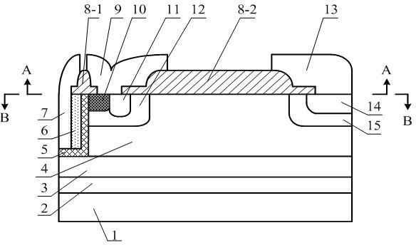
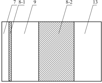
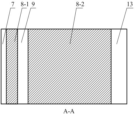
[0014] Such as figure 1 , 2 , 3 and 4, a vertical channel SOI nLDMOS device unit with a p-buried layer, including a p-type semiconductor substrate 1, a buried oxide layer 2, a p-buried layer region 3, and an n-type lightly doped drift region 4 , a gate oxide layer 5, a buried oxide layer 2 covering the p-type semiconductor substrate 1, a p-buried layer region 3 covering the buried oxide layer 2, an n-type lightly doped drift region 4 and a gate oxide layer 5 arranged side by side On the p buried layer region 3, the n-type lightly doped drift region 4 is in contact with the gate oxide layer 5, and the n-type heavily doped polysilicon gate 6 is arranged next to the gate oxide layer 5, and one side of the n-type heavily doped polysilicon gate 6 It is in contact with the gate oxide layer 5.

[0015] On both sides of the top of the n-type lightly doped drift region 4, a p-type well region 12 and an n-type buffer area 15 are respectively embedded, wherein the p-type well region 12...


PUM


Abstract

The invention relates to a longitudinal channel SOI nLDMOS device unit with a p buried layer. The prior products limit the improvements of device structures and electric properties. The longitudinal channel SOI nLDMOS device unit with the p buried layer related by the invention comprises a p-type semiconductor substrate, a buried oxide layer, a p-type buried layer region, a n-type light doping drift region, a p-type well region, a p-type ohm contact region, a n-type source region, a longitudinal oxide layer, a n-type buffering region, a n-type drain region, a field oxygen region, a longitudinal n-type polysilicon gate and a metal electrode lead. The upper part of the device is provided with a deep groove longitudinal gate oxide, two field oxygen layers, a longitudinal n-type polysilicon gate and a metal layer. In the invention, the p-type buried layer region is led-in between the n-type light doping drift region and the buried oxide layer; when the device is in a forward blocking state and a high voltage exists between drain sources, a reverse biased pn (positive negative) node is formed, and the pn node can bear most of the longitudinal withstand voltage of the device, so that the longitudinal voltage-withstand performance of the device is increased, and the thermal stability and thermostability of the device electric property and the heat radiation property of the device are improved.

Description

technical field [0001] The invention belongs to the field of semiconductor technology, and relates to a new structure of a vertical channel SOI (semiconductor on insulating layer) nLDMOS (n-channel lateral double-diffused metal-oxide-semiconductor field-effect transistor) device with a p-type buried layer (BPL). . Background technique [0002] Due to its high integration, high operating frequency and temperature, strong radiation resistance, minimal parasitic effects, low cost and high reliability, SOI LDMOS devices are used as contactless high frequency Power electronic switches or power amplifiers and drivers are widely used in the fields of intelligent power electronics, high-temperature environment power electronics, space power electronics, vehicle power electronics, radio frequency communications, and the Internet of Things. The traditional integrated vertical channel SOI nLDMOS is n - A field oxide layer is formed on the top layer semiconductor; a deep groove is etc...

Claims


Application Information

Patent Timeline
Patent Type & Authority Applications(China)
IPC IPC(8): H01L29/78H01L29/06
Inventor 张海鹏许生根刘怡新吴倩倩孔令军汪洋赵伟立
Owner SERVICE CENT OF COMMLIZATION OF RES FINDINGS HAIAN COUNTY
Why Eureka
Try Eureka