OLED (Organic Light Emitting Diode) device for increasing brightness

A device and metal technology, applied in the field of organic electroluminescence, can solve the problems of large power loss, few research documents, and limitations of the industrialization process of organic light-emitting devices, and achieve the effect of improving the brightness of the device and having little influence on the light transmittance.

Inactive Publication Date: 2011-08-17
西安宙斯光电科技有限公司
View PDF6 Cites 9 Cited by
  • Summary
  • Abstract
  • Description
  • Claims
  • Application Information

AI Technical Summary

Problems solved by technology

[0003] 1. It belongs to the semiconductor range, with low conductivity and large power loss;
[0004] 2. The price of ITO glass or ITO film is high and tends to rise year by year, which restricts the industrialization process of organic light-emitting devices;
[0005] 3. The hole injection ability is not high enough
[0007] However, the application of metal/metal oxide anodes in OLEDs has not attracted enough attention, and there are few research lite

Method used


Image

  • OLED (Organic Light Emitting Diode) device for increasing brightness
  • OLED (Organic Light Emitting Diode) device for increasing brightness
  • OLED (Organic Light Emitting Diode) device for increasing brightness

Examples


Embodiment 1

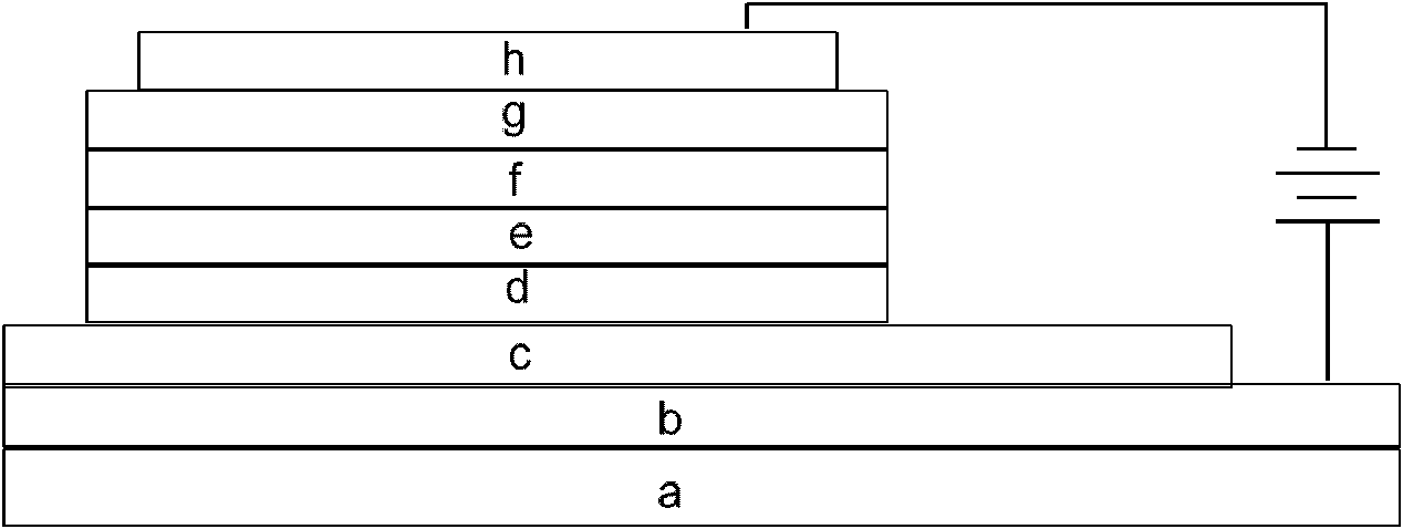
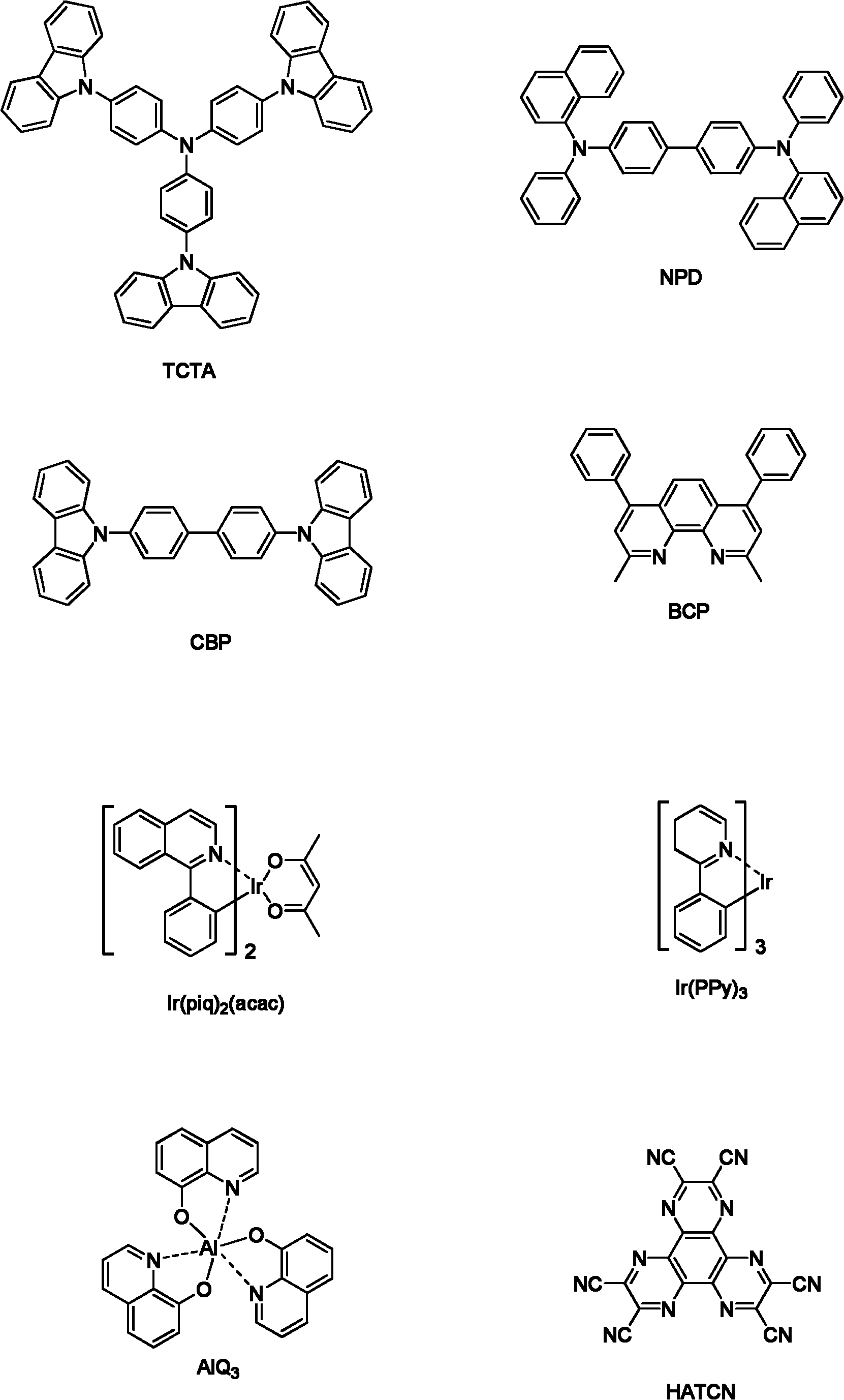
[0037] The flat glass substrate was cleaned with ultrasonic waves in an aqueous solution containing a decontamination agent, rinsed with distilled water and ethanol, and dried. Transfer the substrate to a vacuum thermal evaporation chamber. On the glass substrate, 15nm aluminum is thermally sublimated and evaporated as the anode; then MoO is thermally sublimated and evaporated on the anode in sequence. 3 20nm, NPD60nm, MoO 3 10nm, NPD50nm, CBP and Ir(piq) 2 (acac) 100:8 molar ratio mixed layer 50nm, BCP 15nm, AlQ 3 25nm, LiF 1nm; finally thermal sublimation evaporated aluminum 150nm to form the cathode. The deposition rate is kept at 2 angstroms / s for organic materials, 1 angstroms / s for LiF and molybdenum oxide, and 5 angstroms / s for aluminum. The final device structure is as follows:

[0038] Glass / Al(15nm) / MoO 3 (20nm) / NPD(60nm) / MoO 3 (10nm) / NPD(50nm) / CBP:Ir(piq) 2 (acac)100:8(50nm) / BCP(15nm) / AlQ 3(25nm) / LiF(1nm) / Al(150nm);

[0039] Two layers of MoO 3 The layer...

Embodiment 2

[0041] The flat glass substrate was cleaned with ultrasonic waves in an aqueous solution containing a decontamination agent, rinsed with distilled water and ethanol, and dried. Transfer the substrate to a vacuum thermal evaporation chamber. On the glass substrate, 15nm aluminum is thermally sublimated and evaporated as the anode; then MoO is thermally sublimated and evaporated on the anode in sequence. 3 10nm, SiO 2 1.5nm, MoO 3 10nm, SiO 2 1.5nm, MoO 3 10nm, NPD50nm, CBP and Ir(piq) 2 (acac) 100:8 molar ratio mixed layer 50nm, BCP 15nm, AlQ 3 25nm, LiF 1nm; finally thermal sublimation evaporated aluminum 150nm to form the cathode. The deposition rate is kept at 2 angstroms / s for organic materials, 1 angstroms / s for LiF, silicon oxide and molybdenum oxide, and 5 angstroms / s for aluminum. The final device structure is as follows:

[0042] Glass / Al(15nm) / MoO 3 (10nm) / SiO 2 (1.5nm) / MoO 3 (10nm) / SiO 2 (1.5nm) / MoO 3 (10nm) / NPD(50nm) / CBP:Ir(piq) 2 (acac)100:8(50nm)...

Embodiment 3

[0045] The flat glass substrate was cleaned with ultrasonic waves in an aqueous solution containing a decontamination agent, rinsed with distilled water and ethanol, and dried. Transfer the substrate to a vacuum thermal evaporation chamber. On the glass substrate, 15nm thermally sublimated evaporated aluminum is used as the anode; then thermally sublimated evaporated 10nm titanium cyanine copper, MoO 3 30nm, NPD50nm, CBP and Ir(piq) 2 (acac) 100:8 molar ratio mixed layer 50nm, BCP 15nm, AlQ 3 25nm, LiF 1nm; finally thermal sublimation evaporated aluminum 150nm to form the cathode. The deposition rate is kept at 2 angstroms / s for organic materials, 1 angstroms / s for LiF and molybdenum oxide, and 5 angstroms / s for aluminum. The final device structure is as follows:

[0046] Glass / Al(15nm) / Titanium Copper(10nm) / MoO 3 (30nm) / NPD(50nm) / CBP:Ir(piq) 2 (acac)100:8(50nm) / BCP(15nm) / AlQ 3 (25nm) / LiF(1nm) / Al(150nm);

[0047] where MoO 3 For hole injection and hole transport laye...


PUM

PropertyMeasurementUnit
Total thicknessaaaaaaaaaa
Thicknessaaaaaaaaaa
Brightnessaaaaaaaaaa

Abstract

The invention provides an OLED (Organic Light Emitting Diode) device for increasing brightness, which comprises an anode, a hole adjusting layer and a metal oxide layer arranged on the anode, wherein the hole adjusting layer is arranged in the metal oxide layer, and/or between the metal oxide layer and the anode; and the hole transfer ability of the hole adjusting layer is lower than that of the metal oxide layer. In the invention, anode hole injecting ability and cathode electron injecting ability are balanced by inserting the hole adjusting layer between the metal oxide layer and the metal anode, inserting a hole adjusting layer in a metal oxide hole injecting layer or a metal oxide hole transfer layer, or inserting a hole adjusting layer in the metal oxide hole injecting layer and between the metal oxide hole injecting layer and the metal anode as well; and the brightness of the device is effectively improved, and the OLED device is and simple and easy to implement and has little effect on the light transmittance.

Description

【Technical field】 [0001] The invention relates to the technical field of organic electroluminescence, in particular to metal anodes, hole injection materials and hole transport materials. 【Background technique】 [0002] Organic electroluminescent device (OLED) is a self-luminous, high-brightness, full-color display light-emitting element, and has an attractive prospect in the field of flat-panel display. see figure 1 As shown, the structure of an OLED display device generally includes: a transparent or semitransparent substrate a, an anode b, a hole transport layer c, a light emitting layer (d, e, f), an electron transport layer g and a cathode h. People have rich research results on hole transport layer, light-emitting layer, electron transport layer and cathode materials, but for a long time, the anode is still limited to the traditional ITO conductive glass, and the ITO anode has some obvious disadvantages: [0003] 1. It belongs to the semiconductor range, with low con...

Claims


Application Information

Patent Timeline
IPC IPC(8): H01L51/52H01L51/54H01L51/56
Inventor 闵军辉徐宁宋书清
Owner 西安宙斯光电科技有限公司
Why Eureka
Try Eureka