Aluminum base printed circuit board and preparation method thereof

A printed circuit board, aluminum-based technology, applied in the direction of printed circuit manufacturing, printed circuit, circuit substrate materials, etc., can solve the problems of conductive copper foil etched lines can not be too thin, can not meet the requirements, low adhesion, etc. Overcome easy breakdown by high voltage, achieve high power and high integration, and improve adhesion

Inactive Publication Date: 2011-08-17
任正义
View PDF7 Cites 18 Cited by
  • Summary
  • Abstract
  • Description
  • Claims
  • Application Information

AI Technical Summary

Problems solved by technology

The ordinary metal base printed circuit board in the prior art is made of a thick aluminum plate, which is machined, and then covered with an insulating layer and a conductive copper foil in the processing groove; because the insulating layer is sprayed in a liquid state under normal pressure If it is applied by this method, there will inevitably be defects such as air bubbles and sand holes, which make it easy to be broken down from the defects by high voltages above 500V; the conductive copper foil and the substrate are also bonded with thermally conductive adhesive under normal pressure, resulting in its Insufficient temperature resistance and low adhesion; the corrosion score lines on the conductive copper foil should not be too thin, resulting in the installation and welding of high-power devices on the printed circuit board, single-sided or double-sided welding on the printed circuit board, and large-scale installation. , ultra-large-scale integrated circuit block, unable to meet the requirements of high-power devices and large-scale integrated circuit block micro-lead welding on printed circuit boards

Method used


Image

  • Aluminum base printed circuit board and preparation method thereof
  • Aluminum base printed circuit board and preparation method thereof
  • Aluminum base printed circuit board and preparation method thereof

Examples


Embodiment Construction

[0018] The present invention will be described in further detail below in conjunction with the accompanying drawings and embodiments.

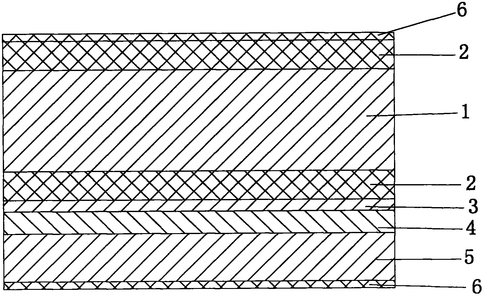
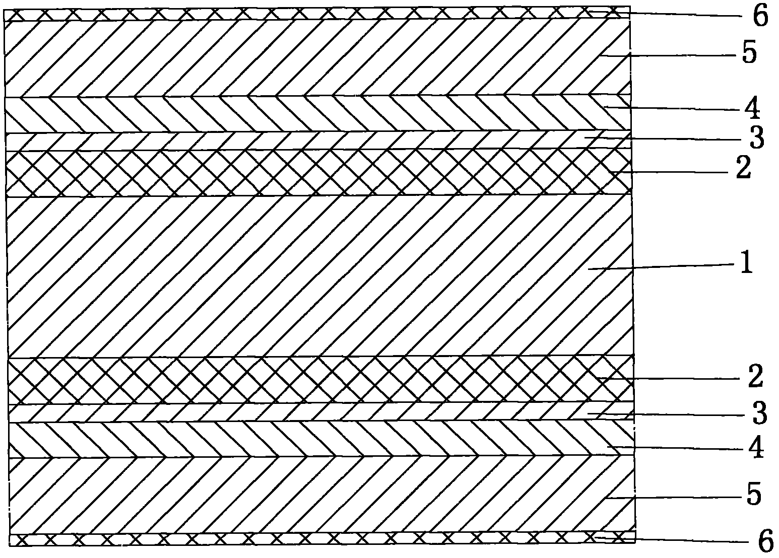
[0019] Such as figure 1 As shown, the aluminum-based printed circuit board of the present invention is provided with an aluminum substrate 1 with a thickness of 1.5 mm to 5 mm when the circuit board is printed on one side. Form dense, high-temperature-resistant, corrosion-resistant and insulating Al2O3 with a thickness of 10 μm to 20 μm 2 o 3 The ceramic insulating layer 2 is coated with a transition layer 3 by a vapor deposition process on the surface of the insulating layer 2 on one side. The vacuum evaporation, vacuum magnetron sputtering or vacuum ion plating process of physical vapor deposition can be used, and the transition layer 3 has a thickness of A 30nm to 80nm chromium, nickel or chromium-nickel alloy film is coated with a copper conductive film 4 with a thickness of more than 300nm on the transition layer 3 by a vapor deposition...


PUM

PropertyMeasurementUnit
thicknessaaaaaaaaaa
thicknessaaaaaaaaaa
thicknessaaaaaaaaaa

Abstract

The invention discloses an aluminum base printed circuit board and a preparation method thereof, which solves the technical problem that the insulating, temperature resistant and withstand voltage values and the scratch fineness of the printed circuit board are improved. An insulating layer is formed on the surface of an aluminum base plate; a copper conducting layer is covered on the insulating layer; and a transition layer and a copper conducting film are arranged between the insulating layer and the copper conducting layer. The preparation method comprises the steps of depositing a transition layer chromium, nickel or chrome-nickel alloy film on the insulating layer of the aluminum base plate, depositing the copper conducting film on the transition layer, and electroplating the copper conducting layer on the copper conducting film. Compared with the prior art, the aluminum base printed circuit board has the advantages that as the aluminum base plate is adopted, aluminum oxide of the aluminum base plate forms the insulating layer, as the nano transition layer is adopted, the adhesive force between the conducting layer and the base plate is greatly improved, and when traditional typographies, such as photograph and chemical corrosion, are adopted, scratch is finer, the manufacture is more precise, and the requirements on large power and high integration to the printed circuit board are satisfied, so that the large power and high integration of the printed circuit board are realized.

Description

technical field [0001] The invention relates to a printed circuit board and a preparation method thereof, in particular to an aluminum-based printed circuit board and a preparation method thereof. Background technique [0002] With the development of computer, communication and aerospace science and technology industries, the demand for high-end printed circuit boards with high power and high integration is becoming increasingly urgent. The ordinary metal base printed circuit board in the prior art is made of a thick aluminum plate, which is machined, and then covered with an insulating layer and a conductive copper foil in the processing groove; because the insulating layer is sprayed in a liquid state under normal pressure If it is applied by this method, there will inevitably be defects such as air bubbles and sand holes, which make it easy to be broken down from the defects by high voltages above 500V; the conductive copper foil and the substrate are also bonded with the...

Claims


Application Information

Patent Timeline
Patent Type & Authority Applications(China)
IPC IPC(8): H05K1/05H05K3/00C23C28/00C23C14/35C25D3/04
Inventor 任正义
Owner 任正义
Why Eureka
Try Eureka